-
FIB & Microelectronic Device Debugging Services
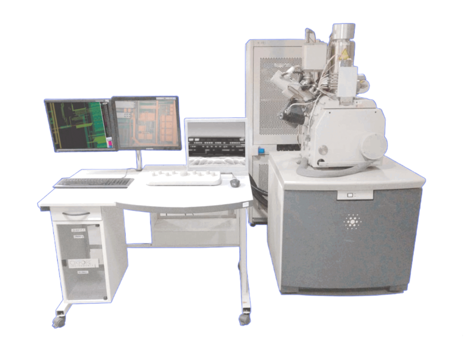
May 12, 2025 | ACS MATERIAL LLCIn today’s fast-paced semiconductor industry, every nanometer counts—and every insight gained from post-fabrication analysis can mean the difference between a successful launch and a costly delay. To meet the evolving needs of engineers and researchers, we are excited to announce the latest addition to our analytical testing catalog: Focused Ion Beam (FIB) & Microelectronic Device Debugging Services.
These specialized services are designed to support chip development throughout its lifecycle, with a particular focus on post-fabrication testing, failure analysis, and design verification. Whether you're investigating a malfunctioning chip, validating design changes, or preparing ultra-thin samples for high-resolution imaging, our advanced capabilities provide the precision and flexibility you need to accelerate development and improve yield outcomes.
Core Capabilities and Services
Decapsulation with Laser and Chemical Etching
Gain access to internal chip structures without compromising functionality. By combining laser ablation and chemical etching, this process enables safe exposure of encapsulated components, setting the stage for in-depth analysis.
Passivation Layer Removal
Expose metal interconnects beneath the chip’s protective passivation layer using precision FIB techniques. This service is critical for signal probing, electrical testing, and localized failure analysis.
Metal Line Connection and Disconnection
Rapidly rewire circuits for debugging or prototyping. With FIB-assisted platinum deposition, we can connect or isolate specific metal lines, helping you validate design modifications without waiting for new mask sets.
Probe Test Point Formation
Create test points directly within complex IC layouts. These points allow you to extract internal signals using a probe station or electron beam, improving visibility into device behavior.
Cross-sectional Analysis
Reveal what lies beneath the surface. Our FIB systems perform precise cross-sectioning at targeted locations, providing vital information on material structure, layer integrity, and manufacturing defects.
TEM Sample Preparation
Produce high-quality lamellae for transmission electron microscopy (TEM) and other high-resolution techniques. Applicable to a wide range of materials, including:
- IC chip regions of interest
- Nanomaterials and coated particles
- Fibrous structures (both cross-sectional and longitudinal)
- Multilayer thin films and interface analysis
As chip architectures grow more intricate and time-to-market shrinks, the ability to rapidly test, analyze, and debug devices is more essential than ever. Our new FIB & Microelectronic Device Debugging Services are here to help you meet that challenge head-on—with the tools, expertise, and reliability your innovation demands.
Ready to learn more or request a service?
Contact our team today to discuss how we can support at contact@acsmaterial.com