-
CVD Graphene for Pt-NP Si Solar Cells - Zhejiang University, 2017
May 21, 2026 | ACS MATERIAL LLCHuang, K., Yan, Y., Yu, X., Zhang, H., & Yang, D. (2017). Graphene coupled with Pt cubic nanoparticles for high performance, air-stable graphene-silicon solar cells. *Nano Energy*.
Nano Energy · 2017
Zhejiang University coupled ACS Material single-layer CVD graphene with Pt cubic nanoparticles to build air-stable graphene-silicon solar cells reaching 10% PCE.
About this research
Researchers at Zhejiang University used commercial single-layer CVD graphene supplied by ACS Material, coupled with cubic platinum nanoparticles, to build air-stable graphene-silicon (Gr-Si) heterojunction solar cells that reach 7% power conversion efficiency (PCE) without antireflection layers and 10% with a spin-coated TiO2 film. The work, published in Nano Energy in 2017 by Huang, Yan, Yu, Zhang and Yang of the State Key Laboratory of Si Materials, demonstrates a new strategy for tuning graphene's Fermi level and work function through physical, rather than chemical, doping, while simultaneously exploiting the plasmonic absorption of noble-metal nanoparticles.
Graphene-silicon Schottky solar cells are a leading test bed for two-dimensional materials in photovoltaics, but pristine CVD graphene has too low a carrier density and work function to drive an efficient junction with n-type silicon. The community has relied on chemical dopants such as HNO3 or AuCl3, which initially raise the built-in field but degrade rapidly in air, etch the graphene, and lower its transparency. Stable doping strategies are therefore an open challenge for any Gr-Si device, including photodetectors, hot-electron emitters and tandem solar architectures. Plasmonic light trapping in thin absorbers is a parallel research direction relevant to silicon photovoltaics broadly, and combining the two on a single graphene electrode is the central idea this paper validates.
The ACS Material single-layer CVD graphene was transferred onto 1–10 Ω·cm n-type ⟨100⟩ silicon wafers using a PMMA carrier and an ammonium persulfate copper etch. After transfer, the stack was annealed at 400 °C in argon to remove residual PMMA and improve the graphene-silicon interface. Raman spectroscopy confirmed the quality of the film: the 2D/G intensity ratio exceeded 2 and no D peak was visible, consistent with a clean monolayer. Cubic Pt nanoparticles with an average diameter of ~7 nm were then synthesized from Pt(acac)2 in a benzyl alcohol/formaldehyde system with PVP as a shape-directing surfactant, redispersed in ethanol, and spin-coated onto the graphene at 1000 rpm to give an optimized ~30% surface coverage. Silver front grids and an In-Ga back contact completed the cells, and a colloidal TiO2 layer was optionally spin-coated as an antireflection film.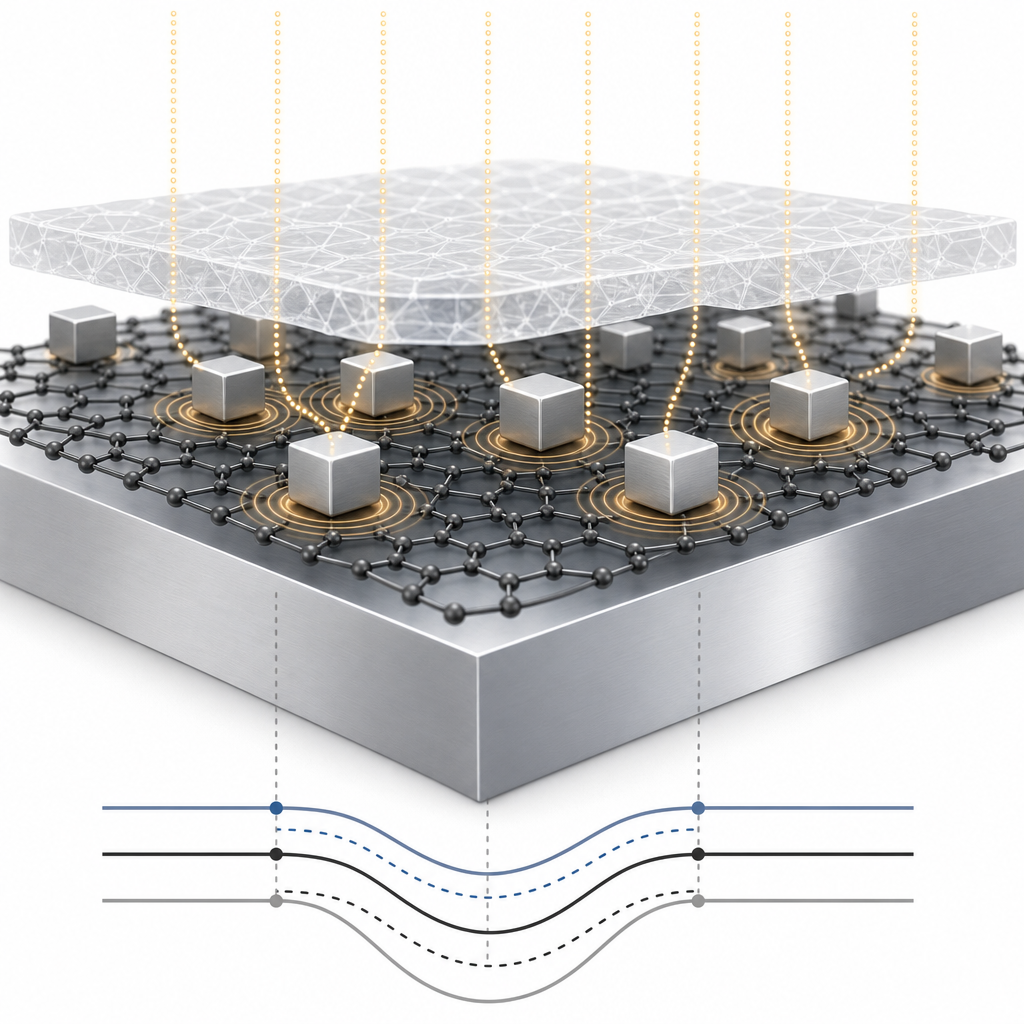 The Pt nanoparticles played two distinct roles. First, their localized surface plasmon resonance increased light absorption in the underlying silicon: cubic particles showed dipole and quadrupole peaks near 300 and 500 nm, and external quantum efficiency rose across the full 300–1100 nm window, with the largest gains in the blue and UV. Reflectance dropped accordingly. Second, the 5.7 eV work function of Pt drove hole transfer into the graphene. Hall measurements on graphene/SiO2 reference samples confirmed an increase in carrier concentration after Pt deposition. Dark J-V analysis showed the saturation current density falling from 4.9 × 10⁻⁶ to 5.0 × 10⁻⁷ A cm⁻², corresponding to a Schottky barrier rising from 850 to 910 meV, in good agreement with the observed Voc gain. Statistical data over twenty cells showed PCE moving from a 3–5% baseline range to a 5–8% range after Pt deposition, with champion pristine devices at 7%. Adding the TiO2 antireflective coating pushed efficiency to 10%. The authors also report a photo-induced doping effect under sunlight illumination, with hot electrons transferring between Pt and graphene to further enhance operating performance. Crucially, unlike chemically doped controls, the Pt-decorated devices showed excellent air stability with no significant degradation.
The study points to a practical recipe for air-stable Gr-Si photovoltaics and, more broadly, for any optoelectronic device that needs simultaneous Fermi-level tuning and light-trapping on a transparent 2D electrode. Adjacent applications include graphene-based photodetectors, hot-carrier solar cells, transparent heaters, and tandem architectures where a doped graphene contact must survive humidity and thermal cycling. The integration of zero-, two- and three-dimensional materials shown here is directly transferable to silicon nanowire arrays, GaAs, and perovskite absorbers, and the same Pt nanocube chemistry could be reapplied to MoS2 or WS2 heterojunctions.
For researchers building similar Schottky or van der Waals devices, the ACS Material single-layer CVD graphene used here is available in the CVD Graphene catalog, including graphene on copper foil suitable for PMMA-based wet transfer onto silicon, quartz, or flexible substrates. The reproducibility of the Schottky barrier shift and the air-stable operation in this study illustrate the value of starting from a uniform monolayer source when the device physics depends on a single, well-defined 2D contact.How ACS Material products were used
- CVD Graphene on Copper Foil (Single-Layer Graphene) (CVD Graphene) — “Commercial single-layer Gr (SLG, bought from ACS Material) and n-type <100> Si wafers (1–10 Ω cm) were used to fabricate the solar cells.”
Product Performance in this StudyThe ACS Material single-layer CVD graphene served as the transparent conductive top electrode and one half of the Schottky junction with n-Si. Raman confirmed high film quality (2D/G > 2, no defect peak), and devices built with this graphene reached 7% PCE after Pt nanoparticle coupling and 10% with a TiO2 antireflective layer.
Related product categories
Frequently asked questionsHow does coupling Pt nanoparticles with graphene improve a graphene-silicon solar cell?
Cubic Pt nanoparticles play two roles. Their localized surface plasmon resonance enhances light absorption in the underlying silicon, raising the short-circuit current across the visible and UV. Their 5.7 eV work function also pulls holes into the graphene, increasing carrier density and lifting the Schottky barrier from 850 to 910 meV, which improves open-circuit voltage and fill factor. The combined effect raises pristine PCE from ~4% to 7%.
Why use CVD single-layer graphene for Schottky junction solar cells on silicon?
CVD single-layer graphene gives a large-area, uniform, atomically thin transparent electrode that forms a built-in field with n-type silicon. Its high transparency lets sunlight reach the Si absorber, while its conductivity carries collected holes to the front contact. A high-quality monolayer, confirmed here by a Raman 2D/G ratio above 2 and no D peak, is essential for reproducible Schottky barriers and reliable doping with metal nanoparticles.
Why is physical doping with Pt nanoparticles more air-stable than chemical doping?
Chemical dopants such as HNO3 or AuCl3 sit on graphene as molecular species that desorb or react with moisture, causing rapid efficiency decay in air. Pt nanoparticles dope graphene through a fixed work-function difference and a stable interfacial charge transfer, with no volatile species. The metal cubes also resist oxidation, so the doping level and Schottky barrier remain constant during prolonged air exposure, preserving device performance.