
Graphene grown by chemical vapor deposition (CVD) sits at the center of much of today's 2D-materials research, because it combines a remarkable set of electrical, optical, and mechanical properties with a route to large, continuous films. Growth needs a metal catalyst (usually copper or nickel)1, a carbon feedstock (typically methane), carrier gases such as hydrogen and argon, and a carefully controlled furnace environment. This article walks through how CVD graphene is grown, how Raman spectroscopy is used to read its quality and layer number, what its sheet resistance and transparency mean for real devices, and how it is transferred from the growth catalyst onto a working substrate.
What Is CVD Graphene?
As interest in graphene has grown on the strength of its structure and remarkable properties — high carrier mobility, mechanical strength, and flexibility — making the material in usable quantities has become the practical bottleneck. Chemical vapor deposition is currently the most widely used route to large-area, continuous graphene films. In CVD, graphene is deposited on a transition-metal substrate that can later be etched away in an acid solution, so the film can be transferred onto an insulating substrate such as silicon dioxide.2 That transferability is what lets CVD graphene be integrated with existing silicon technology, and the low sheet resistance and high optical transparency of graphene on copper make it an attractive candidate for transparent conductive films.
How CVD Graphene Is Grown
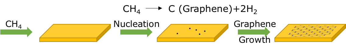
In a typical process, a thin metal foil is placed in a furnace and heated to roughly 900–1000 °C under low pressure. A carbon-bearing gas such as methane is introduced; at the hot catalyst surface the methane decomposes, and the released carbon atoms assemble into a graphene lattice. Copper is the most common catalyst, although nickel and cobalt have also been used.1 The behavior of the two main catalysts is fundamentally different, and understanding that difference explains most of what controls layer number.
Copper has very low carbon solubility, so carbon stays at the surface and growth is essentially self-limiting — once the surface is covered, growth slows, which favors a single layer. Nickel dissolves far more carbon into its bulk at high temperature; on cooling, that carbon segregates back to the surface and can form thick, multilayer graphite rather than monolayer graphene. To keep nickel growth under control, thin nickel films (less than about 300 nm) are evaporated onto a SiO2/Si surface before growth, and a fast cooling rate is used to suppress the formation of extra layers and to help separate the graphene from the substrate.3
Several process variables shape the final quality. Cooling rate and hydrocarbon concentration influence nucleation and growth behavior, and therefore the uniformity of the film.4 The condition of the copper itself matters as well: a poor-quality surface lowers nucleation control, which can be improved by pre-treatment — for example, soaking the copper in dilute acetic acid to remove surface oxide before growth.5 The supply of carbon and hydrogen during growth then tunes how readily the film nucleates and spreads across the surface.
Characterizing CVD Graphene with Raman Spectroscopy
Once the film has been transferred — commonly onto a Si wafer carrying about 300 nm of thermal SiO2, which is smooth, insulating, and compatible with silicon processing2 — Raman spectroscopy is the standard, non-destructive way to assess it. Raman uses monochromatic laser light in the visible, near-infrared, or near-ultraviolet, and reads the light that scatters back from the sample. It is a remarkably versatile probe of graphene: from a single spectrum you can read the number of layers, the density of defects and edges, and the effects of doping and strain.6
How Raman Scattering Works
Almost all of the laser light scatters elastically, at the same frequency as the source — this is Rayleigh scattering, and a Raman instrument filters it out because it carries no vibrational information. A tiny fraction of photons scatter inelastically, exchanging energy with a molecular vibration or lattice phonon; this inelastic effect, first reported by Raman and Krishnan in 1928,7 is what Raman spectroscopy measures.8 When a photon gives up energy to create a vibration, the scattered light is shifted to lower energy (Stokes scattering); when it takes energy from a vibration that is already excited, it is shifted to higher energy (anti-Stokes scattering). Because few vibrations are thermally excited at room temperature, the anti-Stokes lines are much weaker, which is why Raman spectra are normally measured on the Stokes side.9 The interactive diagram below lets you follow a single photon through each of the three processes.
Interactive energy-level (Jablonski) diagram. Switch between Rayleigh, Stokes, and anti-Stokes to see how the scattered photon's energy changes and where the corresponding line sits in the spectrum. Schematic and not to scale.
The G, D, and 2D Bands of Graphene
The Stokes spectrum of graphene is dominated by a few characteristic bands, and their positions, widths, and relative intensities encode the structure of the film.6 The G band (near 1585 cm⁻¹) is the one first-order, always-present feature of any sp2 carbon; its position is sensitive to doping and strain. The D band (near 1350 cm⁻¹ with a green laser) is activated by defects and edges — it is essentially absent in pristine graphene — so its size relative to the G band reflects disorder. That relationship is not a simple proportionality, however: the I(D)/I(G) ratio first rises and then falls as defect density increases, so it must be interpreted with care.10 The 2D band (near 2680 cm⁻¹, historically also called the G′ band) is an overtone of the D-band phonon that needs no defect to appear, which is why it is strong even in clean monolayers.11
The 2D band is the key to counting layers. For monolayer graphene it is a single, sharp, symmetric peak that is taller than the G band — the Raman fingerprint of a monolayer.12 As layers are added, interlayer coupling splits the 2D band into several overlapping components, so it broadens, shifts to higher wavenumber, and becomes less intense relative to the G band, gradually approaching graphite-like behavior. In practice the number of layers is read from the shape of the 2D band together with the I(2D)/I(G) ratio, rather than from the G band alone, and Raman is routinely used to distinguish monolayer, bilayer, and few-layer graphene up to about four layers.13 The simulator below shows how the spectrum evolves as you change the layer number and add a qualitative defect (D-band) contribution.
| Band | Position | Physical origin | What it reveals |
|---|---|---|---|
| G | ~1585 cm⁻¹ | In-plane stretching of sp2 carbon bonds (zone-centre phonon); first order | Always present; shifts with doping and strain |
| D | ~1350 cm⁻¹ | Defect- and edge-activated breathing mode; forbidden in pristine graphene | Disorder, defects and edges; I(D)/I(G) gauges defect density |
| 2D (G′) | ~2680 cm⁻¹ | Overtone of the D-band phonon; needs no defect | Layer number, from its shape and the I(2D)/I(G) ratio |
Positions are approximate, measured near 532 nm excitation; the D and 2D bands shift with laser wavelength.
Interactive Raman spectrum. Choose 1–4 layers and adjust the defect slider to watch the G, D, and 2D bands change; the readouts report the height ratios and the 2D position and width. Peak positions shift with laser wavelength, strain, and doping, so the values shown are representative rather than absolute.
Sheet Resistance and Transparency
For transparent-electrode applications, the figure of merit is the trade-off between sheet resistance and optical transparency, and a high sheet resistance is one of the limits on graphene-based electrodes in organic electronic devices.14 Undoped, single-layer graphene is a one-atom-thick crystal with a sheet resistance of roughly 6 kΩ/sq at about 98% transparency. Graphene grown by CVD on copper has been reported at around 350 Ω/sq while keeping about 90% transparency — a far better transparency-to-resistance balance that is what makes CVD graphene practical for transparent conductive films.15 Adding layers lowers the sheet resistance further: each additional layer contributes in parallel, so resistance drops as layers stack, while transparency decreases.16
Transferring Graphene: the PMMA Support Layer
Because a graphene monolayer is only one atom thick, it needs mechanical support during transfer once the metal catalyst is etched away. Poly(methyl methacrylate), or PMMA, is the most common temporary support: it is spin-coated onto the graphene — typically tens to a few hundred nanometers thick — to keep the film from tearing or folding, after which the metal is etched and the PMMA/graphene stack is moved onto the target substrate.17 ACS Material's Trivial Transfer™ Graphene is built around exactly this idea, packaging the film with a support layer so it can be floated onto an arbitrary substrate.
The main drawback of PMMA is residue: a thin polymer layer can remain on the graphene surface and alter its intrinsic properties. Rinsing the supported film in distilled water reduces contamination before transfer, and the PMMA is then dissolved with an organic solvent such as acetone. A clean Raman spectrum — sharp G and 2D bands with little D intensity — is a good first indicator that the polymer has been removed, but trace residue can persist below the Raman detection limit. More sensitive methods, such as isotope labeling of the PMMA combined with time-of-flight secondary ion mass spectrometry (ToF-SIMS),1819 can detect what Raman misses, and ToF-SIMS is a useful complement to Raman for characterizing surface chemistry and contamination on 2D materials.20
Outlook
CVD remains the most scalable, cost-effective route to large-area, high-quality graphene for research and devices. Its ability to produce continuous monolayer films on inexpensive metal foils — and to transfer them onto silicon, glass, or flexible substrates — has driven a decade of progress in transistors, transparent conductors, sensors, and barrier coatings. As growth uniformity, defect control, and clean transfer continue to improve, CVD graphene moves steadily from a laboratory material toward a manufacturable one.
CVD Graphene from ACS Material. ACS Material supplies CVD-grown graphene and the materials needed to put it to work:
- CVD Graphene — monolayer and few-layer films on copper, nickel, and target substrates.
- Trivial Transfer™ Graphene — graphene with a support layer for easy transfer onto your own substrate.
- Transparent Conductive Film — graphene-based films for transparent-electrode applications.
- Graphene Series — the full range of graphene and graphene-derivative products.
Frequently Asked Questions
What is CVD graphene, and what does “CVD” stand for?
CVD graphene is graphene grown by chemical vapor deposition. “CVD” stands for Chemical Vapor Deposition — a bottom-up method in which a carbon-rich gas, typically methane, decomposes at high temperature on a metal catalyst and assembles into a graphene film.
How does the CVD growth process work?
A carbon-bearing gas such as methane is decomposed on a heated metal substrate, most often copper, at roughly 900–1000 °C. Carbon atoms assemble into a graphene layer on the surface; after cooling, the film can be transferred onto another substrate such as silicon (or silicon dioxide) for use in electronics, sensors, and transparent conductors.
Why is copper the most common catalyst, and when is nickel used?
Copper has very low carbon solubility, so growth is surface-limited and tends to stop at a single layer — ideal for monolayer graphene. Nickel dissolves much more carbon, which segregates on cooling to form multilayers, so thin nickel films (under about 300 nm) and fast cooling are used to limit extra layers.
What can Raman spectroscopy tell you about graphene?
Raman is the standard, non-destructive probe for graphene. The shape of the 2D band and the I(2D)/I(G) ratio indicate the number of layers, the D band reveals defects and edges, and shifts in the G and 2D bands report doping and strain.
How many layers can Raman distinguish?
Raman reliably distinguishes monolayer, bilayer, and few-layer graphene — up to about four layers — from the 2D-band shape: a single sharp 2D peak for a monolayer that broadens, upshifts, and splits into components as layers are added, approaching graphite-like behavior.
What is the PMMA layer for, and how is the residue removed?
PMMA is spin-coated as a temporary mechanical support so the graphene does not tear or fold during transfer after the metal catalyst is etched. It is later dissolved in an organic solvent such as acetone; trace residue can be checked by Raman and, more sensitively, by ToF-SIMS.
Is CVD a top-down or a bottom-up method?
Bottom-up. CVD builds graphene atom by atom from a gas-phase carbon source, in contrast to top-down methods such as mechanical or liquid-phase exfoliation that break bulk graphite down into thin flakes.
Why is high-quality graphene expensive?
Producing large-area, low-defect graphene requires high temperatures, tightly controlled conditions, high-purity catalysts, and a careful transfer step. Each of these adds cost, and yield losses during transfer make defect-free films harder to deliver at scale.
References
This article is provided by ACS Material LLC for educational purposes only. It concerns graphene grown by chemical vapor deposition (CVD); the idealized, single-layer figures cited here — for example a sheet resistance near 6 kΩ/sq at about 98% transparency, or about 350 Ω/sq at roughly 90% transparency — are literature benchmarks that real transferred, doped, or multilayer films will not match exactly. For the specifications and safe handling of any particular product, consult its datasheet and Safety Data Sheet (SDS). The interactive diagrams on this page are schematic teaching tools, not quantitative or predictive design software.