-
DNA-Au Nanoparticle Colloidal Crystals - Northwestern, 2022
May 20, 2026 | ACS MATERIAL LLCWang, S., Lee, S., Du, J. S., Partridge, B. E., Cheng, H. F., Zhou, W., Dravid, V. P., Lee, B., Glotzer, S. C., & Mirkin, C. A. (2022). The emergence of valency in colloidal crystals through electron equivalents. *Nature Materials*. https://doi.org/10.1038/s41563-021-01170-5
Nature Materials · 2022
Northwestern University researchers use 10 nm and 1.4 nm gold nanoparticles with DNA to build nine colloidal crystal phases, including three new low-symmetry lattices.
About this research
Researchers at Northwestern University, working with colleagues at the University of Michigan and Argonne National Laboratory, used DNA-functionalized gold nanoparticles to assemble nine distinct colloidal crystal phases, including three low-symmetry lattices that had never before been observed in colloidal systems. By treating 10 nm Au nanoparticles as programmable atom equivalents (PAEs) and 1.4 nm Au nanoparticles as mobile electron equivalents (EEs), the team showed that anisotropic distributions of small particles around larger ones can break lattice symmetry. The result is a rational route to body-centred tetragonal (BCT), high-pressure gallium (HP-Ga) and triple double-gyroid superlattices from isotropic building blocks.
Colloidal crystal engineering with DNA has emerged as a powerful method to control nanoparticle superlattice symmetry, lattice parameters and crystal habit independent of particle composition. However, isotropic spherical building blocks naturally favour close-packed phases such as FCC and BCC, leaving complex, low-symmetry architectures difficult to access. The classical concept of valence electrons explains why molecules and atomic crystals can adopt low-symmetry geometries, and recent work suggested that small DNA-grafted nanoparticles could play an analogous role for larger PAEs. This paper directly tests whether such electron equivalents can be programmed to dictate the symmetry of a PAE lattice, opening the door to phases relevant for photonics, metamaterials, plasmonics and catalysis.
The PAEs and EEs were prepared by modifying 10 nm and 1.4 nm gold nanoparticles with single-stranded, propylthiolated DNA, yielding particles bearing roughly 160 and 15 DNA ligands, respectively. The ssDNA-modified particles were then duplexed with linker strands containing six-base sticky-end overhangs that enable selective hybridization between PAEs and EEs. By systematically varying the EE/PAE stoichiometry and the number of input linker strands, the authors tuned the density of sticky ends on each particle type. This allowed precise control over the strength and spatial distribution of DNA-mediated bonds. Synchrotron small-angle X-ray scattering (SAXS) at Argonne's Advanced Photon Source, low-angle annular dark-field electron microscopy and molecular dynamics simulations were used to identify the resulting structures and to quantify EE delocalization, diffusivity and coordination geometry within each lattice.Northwestern’s programmable colloidal crystals reveal how the ratio of small “electron equivalent” particles to large “programmable atom” particles dictates the final lattice symmetry — a milestone in DNA-directed nanomaterial design. Resolving the sub-2 nm electron equivalents within these superlattices demands an ultra-thin, low-background imaging support: the few-layer CVD graphene membrane used for structural characterization in this study was supplied by ACS Material. Explore our CVD Graphene on Copper Foil and TEM Grids to enable high-resolution electron microscopy of your own nanoscale assemblies.
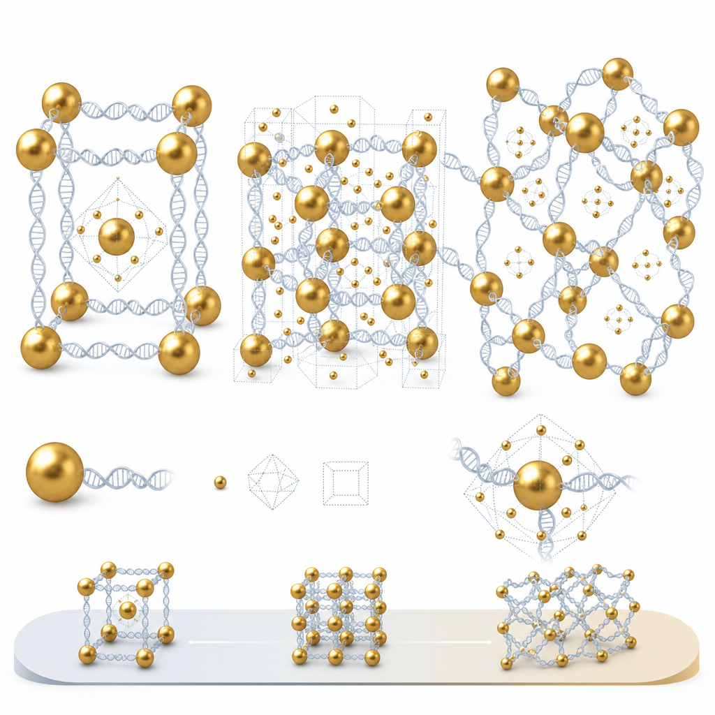
Nine equilibrium crystalline phases formed spontaneously: FCC, BCC, Frank–Kasper A15, two BCT variants, simple hexagonal, HP-Ga, triple double-gyroid and simple cubic. Three of these – BCT, HP-Ga and triple double-gyroid – are reported here for the first time in colloidal crystals; two have elemental analogues, while the gyroid phase has no known natural equivalent. Simulated and experimental SAXS structure factors agree closely across all nine phases. The PAE-core packing fraction varies systematically from below 1‰ in the FCC phase up to almost 10‰ in the simple cubic phase as the EE/PAE stoichiometric ratio decreases. Quantitative analysis shows that PAE–EE surface-to-surface spacings remain nearly constant across all phases and match the length of two hybridized DNA linkers. EE coordination environments evolve from a 24-coordinated rhombicuboctahedron in FCC to an 8-coordinated cube in simple cubic, mirroring the way valence electrons organize around atoms. The phases fall into three classes – metallic, tetrahedral and high-coordination – distinguished by EE delocalization, sphericity of the EE shell, and diffusivity. Two enantiotropic phase transformations driven by EE redistribution upon thermal treatment were also demonstrated.
These findings establish a general design framework for low-symmetry colloidal crystals built from simple, isotropic spherical particles, expanding the toolbox beyond shape-anisotropic building blocks and polyhedral templates. Potential applications include photonic crystals with engineered band gaps, plasmonic metamaterials, structural colour, anisotropic catalysts and templated porous materials. The triple double-gyroid lattice, in particular, has no atomic analogue and may exhibit unusual optical and transport properties. The combination of programmable DNA bonding with mobile electron-equivalent particles also offers a platform to study fundamental questions about valency, coordination chemistry and phase transitions in soft matter, including reconfigurable crystals that respond to temperature or sequence cues.The gold nanoparticles used as building blocks in this study were sourced elsewhere (10 nm from Ted Pella; 1.4 nm Nanogold from Nanoprobes). ACS Material's contribution was in the structural characterization: to image the silica-embedded crystals containing sub-2 nm electron-equivalent particles, the authors needed a support that would not bury such small features under background. Conventional ~20 nm amorphous carbon films work for the larger 10 nm particles, but for grids carrying the 1.4 nm EEs the team instead wet-transferred a three-to-five-layer CVD graphene membrane (grown on copper foil, ACS Material) onto the grid. Graphene's single-to-few-atom thickness and low atomic number give an almost transparent, low-noise background, letting low-angle annular dark-field STEM resolve the faint EE positions that define each lattice. For groups doing high-resolution TEM/STEM of nanoparticles, 2D materials, soft matter or beam-sensitive specimens, few-layer CVD graphene on Cu is a practical, transferable support membrane and graphene-liquid-cell window — and was the enabling characterization material behind the structural analysis reported here.
How ACS Material products were used
- CVD Graphene on Copper Foil (3–5 layers) (Graphene Series) — “a graphene membrane comprising three to five layers (grown by chemical vapour deposition on Cu foil, ACS Material) was coated onto the grid using a wet transfer method”
Product Performance in this Study
The 3–5 layer CVD graphene served as the TEM support membrane for the most demanding samples in the study — cross-sections containing the 1.4 nm electron-equivalent particles, which conventional carbon films could not image cleanly. Wet-transferred onto the grid, the graphene provided an ultrathin, low-background window that let low-angle annular dark-field STEM resolve the individual EE positions used to determine the coordination geometry of each colloidal-crystal phase.
Related product categories
Frequently asked questions
How do electron equivalents break symmetry in DNA-mediated colloidal crystals?
Small 1.4 nm gold nanoparticles bearing only about 15 DNA strands act as mobile electron equivalents that diffuse around larger 10 nm programmable atom equivalents. Their anisotropic spatial distribution and tunable stoichiometry produce well-defined coordination geometries around each large particle, much as valence electrons surround an atom. This breaks the close-packed symmetry favoured by isotropic spheres and enables low-symmetry phases such as BCT and HP-Ga.
What new colloidal crystal phases were discovered in this study?
Out of nine equilibrium phases formed, three are reported as colloidal crystals for the first time: body-centred tetragonal (BCT), high-pressure gallium (HP-Ga) and a triple double-gyroid lattice. BCT and HP-Ga have known elemental analogues, while the triple double-gyroid structure has no natural atomic equivalent. The remaining phases include FCC, BCC, Frank–Kasper A15, simple hexagonal and simple cubic, all assembled from the same isotropic spherical gold nanoparticle building blocks.
Why use CVD graphene as a TEM support membrane instead of a carbon film?
A few-layer CVD graphene membrane is only a fraction of a nanometre thick and made of low-atomic-number carbon, so it adds far less background scattering than a conventional ~20 nm amorphous carbon film. That matters when the features of interest are tiny: in this study the 1.4 nm electron-equivalent particles would be lost against a thick carbon background, whereas a 3–5 layer graphene window let low-angle annular dark-field STEM resolve their positions. Graphene supports (and graphene liquid cells) are widely used for high-resolution imaging of nanoparticles, 2D materials and beam-sensitive or hydrated specimens for this reason. ACS Material supplies continuous CVD graphene on copper foil in 1, 2, 3–5 and 6–8 layer grades that can be wet-transferred onto TEM grids and other substrates.