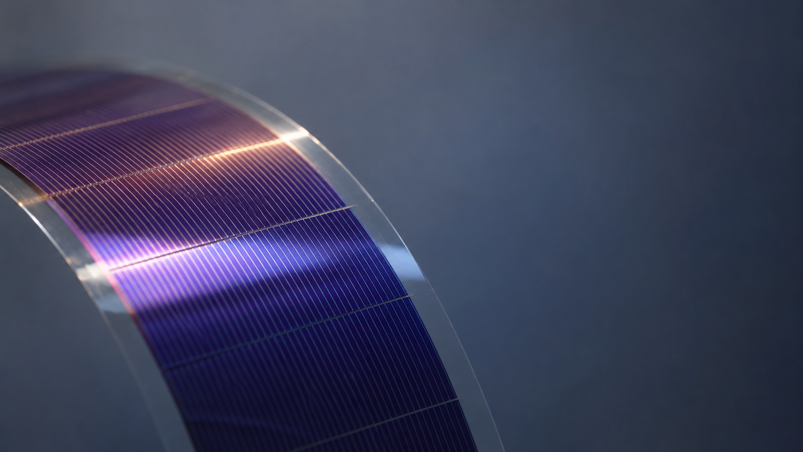
Most solar panels are rigid slabs of silicon behind glass. There is a lighter, bendable alternative — the organic solar cell, whose light-absorbing film is printed from carbon-based inks only a few hundred nanometers thick. As researchers pushed these printed cells toward higher efficiency and genuine flexibility, they kept hitting the limits of the conventional materials surrounding that ink, and time after time the answer turned out to be another form of carbon. This article looks at how graphene and its chemical relatives have worked their way into nearly every layer of the organic solar cell — and how close that has brought printed, indium-free photovoltaics to the performance of their rigid cousins.
Short answer: Organic solar cells (OSCs) turn sunlight into electricity using thin, printable films of carbon-based semiconductors instead of rigid silicon wafers. Graphene — a single sheet of carbon atoms that is transparent, conductive, flexible, and chemically robust — can step into almost every layer of that stack: as the see-through electrode that replaces brittle indium tin oxide (ITO), as the hole- or electron-transport layer that shuttles charge to the contacts, and even inside the light-absorbing layer as quantum dots. No single one of these roles yet makes a graphene-based cell outperform the best silicon or ITO-based cells on efficiency alone, but together they point toward solar cells that are lighter, bendable, cheaper to print, and free of scarce indium.1
How organic solar cells work — and where ITO becomes a problem
A solar cell converts light into electricity through the photovoltaic effect: a photon is absorbed, an electron is promoted to a higher-energy state, and the two contacts of the device sweep the freed charges out as current. In a conventional cell the absorber is crystalline silicon. In an organic solar cell — also called an organic photovoltaic (OPV), plastic, or polymer solar cell — the absorber is a blend of carbon-based semiconductors that can be dissolved into an ink and printed as a film only a few hundred nanometers thick. That thinness is the whole appeal: OSCs can be lightweight, semi-transparent, mechanically flexible, and manufactured by roll-to-roll coating rather than high-temperature wafer processing.1
Inside a typical device the photoactive film is a bulk heterojunction — an intimately mixed network of an electron-donor material and an electron-acceptor material. When light creates a bound electron–hole pair (an exciton), it splits at the donor–acceptor interface; the electron travels through the acceptor network to one contact while the hole travels through the donor network to the other. Thin interlayers on each side, the hole-transport layer (HTL) and electron-transport layer (ETL), make each contact selective so that the right carrier is collected and the wrong one is blocked. Decades of work on new donor and acceptor molecules have pushed laboratory OSC efficiencies past 20 %, turning them from a curiosity into a credible thin-film technology.2
For any of this to work, at least one electrode must let light in. The industry-standard transparent conductor is indium tin oxide (ITO), which combines good conductivity with high visible transparency. But ITO has two weaknesses that matter enormously for the flexible, low-cost future OSCs promise: indium is a scarce, price-volatile element, and ITO is a ceramic that cracks when bent, making it a poor fit for roll-to-roll and flexible devices.3 That single limitation is what first drew researchers to graphene — and once graphene was in the device, they found it could do far more than replace ITO.
Four jobs graphene can do in an organic solar cell
“Graphene” in photovoltaics is really a family of related materials: pristine single-layer graphene grown by chemical vapor deposition (CVD), solution-processed graphene oxide (GO) and reduced graphene oxide (rGO), and zero-dimensional graphene quantum dots (GQDs). Each form brings a different mix of conductivity, transparency, work function, and solubility, and that versatility is exactly why graphene keeps appearing in every part of the OSC stack.1 Broadly, graphene-related materials play four roles: they serve as the transparent electrode, as the hole-transport layer, as the electron-transport or interfacial layer, and as a component inside the photoactive layer itself. Beyond charge handling, their dense two-dimensional sheets also act as diffusion barriers that shield the device from oxygen and moisture, which can improve operating stability.1
The most mature of these roles is the transparent electrode, so it is worth seeing directly how graphene stacks up against the ITO it aims to replace. Two properties always trade off against each other: sheet resistance (lower is better for collecting current) and optical transmittance (higher is better for letting light reach the absorber).
| Property | Indium tin oxide (ITO) | Graphene electrode |
|---|---|---|
| Raw-material supply | Indium is scarce and price-volatile | Carbon is abundant and low-cost3 |
| Mechanical flexibility | Brittle ceramic; cracks on bending | Flexible; survives repeated bending4 |
| Sheet resistance vs. transparency | ~10–30 Ω/sq at >85 % transmittance | CVD film ~230 Ω/sq at 72 %; improves with doping4,5 |
| Fundamental limit | Set by a doped oxide network | Set by graphene’s intrinsic conductivity ratio3 |
| Large-area manufacturing | Vacuum sputtering | Roll-to-roll CVD and transfer demonstrated at 30-inch scale6 |
| Work-function tunability | Limited | Tunable by doping and functionalization5 |
The table makes the trade clear: graphene is not yet as conductive-at-high-transparency as the best ITO, but it wins decisively on abundance, flexibility, and compatibility with large-area printing — the properties that make OSCs worth pursuing in the first place. The interactive tool below lets you feel that trade-off directly.
The transparent electrode: replacing ITO
The first demonstrations used solution-processed graphene. Spin-coating a dispersion of chemically derived graphene, then reducing it to restore conductivity, produced transparent anodes on which small-molecule organic cells could be built directly — proof that a printed carbon film could replace a sputtered oxide, even if early sheet resistance and fill factor lagged ITO.7 Large-area ultrathin films of reduced graphene oxide gave the same idea a flexible, solution-cast form,8 and rGO transparent electrodes were soon integrated into working OPV devices, reaching around 0.8 % efficiency — modest, but a genuine indium-free cell.9
The breakthrough for quality came from CVD-grown graphene. Because a CVD film is continuous rather than a patchwork of overlapping flakes, it is far smoother (surface roughness around 0.9 nm) and more conductive: sheet resistance fell to roughly 230 Ω/sq at 72 % transmittance. Crucially, when researchers built organic cells with CVD-graphene and ITO electrodes side by side on flexible PET, the graphene devices delivered comparable efficiency — about 1.18 % versus 1.27 % — and kept working when bent, where the ITO control failed.4 That flexibility, not raw efficiency, was the headline result.
From there the field attacked graphene’s main weakness — sheet resistance that is still higher than ITO’s at the same transparency. There is a genuine physical ceiling here, set by the ratio of graphene’s electrical to optical conductivity, which caps how conductive a film of a given transparency can be.3 Within that ceiling, three levers help: chemical doping raises carrier density and lowers sheet resistance for a given number of layers,5 stacking a few layers trades transparency for conductivity — multilayer CVD-graphene anodes have driven efficient bulk-heterojunction cells,10 and a typical multilayer film (around 374 Ω/sq at 84 % transmittance) yields roughly 1.17 % efficiency11 — and hybridizing graphene with metal nanowires or carbon nanotubes combines their strengths.12 Similar percolation-network physics governs competing indium-free conductors such as silver-nanowire meshes, which is why graphene is usually benchmarked against them.13,14 Careful studies have also shown that the electrode’s morphology and the transport layer placed on top of it matter as much as the sheet resistance itself.15 The maturing of roll-to-roll CVD and transfer — famously to 30-inch scale — is what makes graphene electrodes plausible for manufacturing rather than lab curiosities.6,16 High-quality monolayer graphene of the kind used in these studies is available as CVD graphene films.
Graphene oxide as a hole-transport layer
Between the anode and the photoactive blend sits the hole-transport layer, whose job is to collect holes efficiently while blocking electrons. The long-time standard, PEDOT:PSS, works well but is acidic and hygroscopic, and over time it corrodes the electrode and degrades the cell. In a landmark 2010 result, a thin film of solution-processed graphene oxide was inserted as the HTL in a P3HT:PCBM cell; because GO is electrically insulating in-plane but conducts holes vertically and has a large band gap that blocks electrons, it cut recombination and leakage and raised efficiency to values comparable with PEDOT:PSS — without the acidity.17 That paper turned GO into one of the most-studied interfacial materials in organic electronics.
Refinements followed quickly. Combining GO with PEDOT:PSS in a double-decked HTL captured the strengths of both layers and lifted efficiency above either alone (about 4.3 % versus roughly 2.8 % and 3.6 % for the individual layers) while improving stability.17 Reducing and chemically tailoring the sheets solved GO’s biggest limitation — that its work function and conductivity depend sensitively on oxidation. Fluorinated reduced graphene oxide, for example, provided an efficient and notably more stable hole-transport layer,18 and the same reasoning drives interest in printable graphene inks: an inkjet-printed graphene HTL improves selective hole extraction and blocks the metal diffusion and recombination that shorten device life.19 The recurring theme is energy-level matching — the electrode and interlayer work functions must line up with the donor’s levels for holes to flow with minimal loss, which is why the precise electronic structure of graphene films and their alignment with organic semiconductors is studied so carefully.20 Hybrid carbon electrodes that fold the hole-transport function into the contact stack — a carbon-nanotube/graphene film paired with a thin oxide layer — are a recent extension of the same idea.21
Reduced graphene oxide, quantum dots, and interfacial layers
On the other side of the device, the electron-transport or cathode interlayer must collect electrons and block holes — the mirror image of the HTL’s task. Here the key variable is work function: an interlayer with a low work function pulls electrons out efficiently. Graphene derivatives are attractive because their work function can be tuned. Zero-dimensional carbon quantum dots, produced in a single large-scale synthesis step, have served as efficient cathode interlayers in polymer solar cells, improving electron extraction at low cost.22 Reduced graphene oxide and graphene quantum dots have also been folded into the electron-transport side of inverted cells, blended with metal-oxide transport layers to improve electron extraction and carrier lifetime.1
What makes graphene-family interlayers powerful is that the same material can be nudged to do opposite jobs. Oxidize it and raise its work function, and it extracts holes; reduce or functionalize it to lower the work function, and it extracts electrons. Combined with their solution processability and their role as compact barriers against moisture and oxygen, this tunability lets a single, cheap material class handle both interfaces of a printed cell — a real simplification for manufacturing.1
Graphene inside the active layer
The most ambitious role puts graphene into the light-absorbing blend itself. Bulk-graphene sheets are poor absorbers, but graphene quantum dots — nanometer fragments confined enough to open a tunable band gap — behave like designable molecular semiconductors. In an early demonstration, GQDs blended with a conjugated polymer worked as electron acceptors and markedly improved photovoltaic performance compared with larger graphene sheets, hinting at inexpensive fullerene-free acceptors.23 Related work showed that electrochemically prepared, green-luminescent GQDs could serve as electron acceptors in polymer cells,24 and that tailoring the GQD precursor — for example deriving dots from double-walled carbon nanotubes — raised short-circuit current and efficiency.25 Because their size sets their optical gap, GQDs can also broaden light harvesting: used as downshifting or light-managing layers, they have boosted efficiency in hybrid graphene-silicon cells to around 13 %.26
More recent designs use GQDs as one ingredient in multi-component blends, where amine-functionalized dots help extend absorption and improve charge transport in quaternary polymer cells.27 The luminescent GQD demonstrations trace back to the recognition that graphene, cut down to the quantum scale, is itself a tunable photovoltaic material rather than merely a contact.28 These active-layer roles remain less efficient than the best non-fullerene acceptors, but they are a striking illustration of how one element — carbon — can supply the electrode, the interlayers, and the absorber of a single device.
The bigger picture: efficiency, flexibility, and stability
How far has all of this pushed real devices? On raw efficiency, graphene components have not overtaken the best conventional OSCs, but they have closed much of the gap: reviews report that OSCs incorporating polymer-modified graphene as a transparent electrode have exceeded 15 % efficiency, within reach of ITO-based cells.1 Where graphene wins outright is on the properties that make organic photovoltaics distinctive. Its flexibility enables cells that survive repeated bending, its abundance removes the dependence on scarce indium, and its dense two-dimensional structure acts as a barrier that can improve operational stability — all while remaining compatible with the low-temperature, solution-based, roll-to-roll printing that gives OSCs their cost advantage.4,28
The lessons learned in organic cells carry over directly to neighboring technologies: graphene materials play the same electrode and interfacial roles in dye-sensitized and perovskite solar cells, and progress in one area feeds the others.29 The honest assessment is that graphene is not a single silver bullet for organic photovoltaics but a remarkably versatile toolkit — one material family that can be tuned to serve as the window, the wiring, and even the light-harvester of a printed solar cell.30 As the quality of large-area graphene continues to improve and its work function becomes easier to control, its role in the flexible, indium-free solar cells of the future looks set to grow.
ACS Material supplies research-grade graphene for exactly this kind of work, including CVD graphene films and the broader graphene product series. For the fundamentals behind everything above, see our complete guide to graphene.
References
This article is provided by ACS Material LLC for educational purposes and describes the use of graphene and graphene-related materials — including graphene oxide, reduced graphene oxide, and graphene quantum dots — in organic solar cells (organic photovoltaics). Power conversion efficiencies, sheet resistances, transmittances, work functions, and other figures are representative values drawn from the referenced studies; results for any specific device depend on the materials, device architecture, processing, and measurement conditions used, and real devices will differ from idealized descriptions. The interactive tool is a schematic teaching aid based on the stated model — an idealized transparent-electrode comparison using a per-layer optical absorption of about 2.3 % and the Haacke figure of merit, which weighs optical transmittance against sheet resistance — and is not predictive design software. Consult product datasheets and safety data sheets for material specifications and handling guidance.