Graphene transfer is the step that moves a graphene film off the metal foil it was grown on and onto the substrate where it will actually be used. It is deceptively decisive: the growth recipe sets the graphene’s intrinsic quality, but the transfer determines how much of that quality survives — whether the film arrives continuous and clean, or cracked, wrinkled, and contaminated. This guide explains why transfer is necessary, walks through the main methods (wet PMMA, dry tape and stamp, and etch-free electrochemical), compares their trade-offs, and shows how to get a clean result.
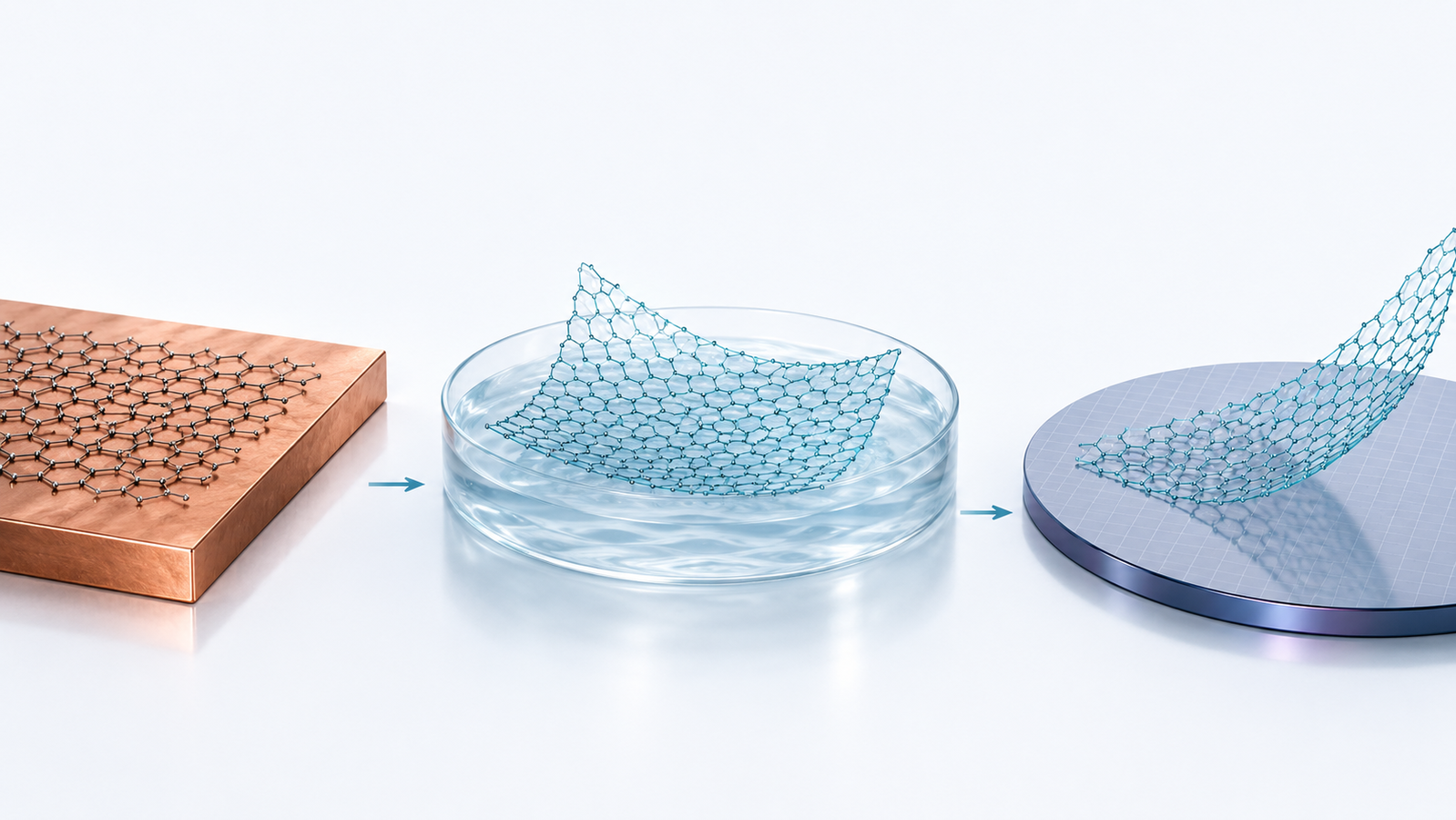
Short answer: graphene transfer relocates a CVD-grown graphene film from its growth metal (usually copper) onto a target substrate such as SiO2/Si, quartz, glass, or PET. Two families dominate. In wet transfer, a polymer support (typically PMMA) holds the film together while the metal is etched away and the film is floated onto the new surface. In dry transfer, a tape or elastomer stamp (thermal release tape, PDMS) picks the film up and presses it down. A third, etch-free route uses electrochemical bubbling to peel the film off and reuse the metal. The recurring enemies are cracks, wrinkles, and polymer residue. ACS Material’s Trivial Transfer® Graphene removes the hardest steps — the film arrives PMMA-supported and ready to float onto your substrate with only tweezers and DI water.
Why graphene has to be transferred
The highest-quality large-area graphene is made by chemical vapor deposition (CVD), in which methane is decomposed at around 1000 °C over a metal catalyst — usually copper, sometimes nickel or platinum — that templates the carbon atoms into a continuous honeycomb sheet. The catalyst is essential to growth, but a metal foil is useless as a working surface: it is opaque and electrically conductive, so it shorts out any device built on it. To make a transistor, a transparent electrode, a sensor, or a membrane, the graphene has to end up on an insulating or transparent substrate — SiO2/Si wafers for microelectronics, quartz or glass for optics, or PET and other polymers for flexible devices. Transfer is the bridge between the two: it removes the growth metal and relocates the atom-thin film onto the substrate where it will actually be used. For a broader primer on the material itself, see ACS Material’s complete guide to graphene.
What makes transfer hard
A graphene sheet is a single atom thick, has almost no bending stiffness of its own, and clings to surfaces only through weak van der Waals forces. Moving it intact is therefore genuinely difficult, and three failure modes dominate.
Cracks and tears. With nothing to support it, an unsupported monolayer fractures the instant it is handled. This is why a temporary polymer carrier is almost always applied first: it lends the film the stiffness it lacks on its own. Polymer-supported transfer produces dramatically fewer cracks and tears than handling bare graphene, while preserving high optical transmittance and conductivity over large areas.1
Wrinkles and folds. Differences in thermal expansion between graphene and its carrier, together with the surface tension of liquids during drying, can buckle the film into wrinkles and folds that scatter carriers and create weak points.
Residue and doping. The carrier polymer never washes off completely. A residual layer a few nanometers thick typically remains and electrically dopes the graphene, lowering carrier mobility; etchant ions and adsorbed water can leave the film p-doped as well. Because so much of the final device performance is decided here rather than at growth, transfer is widely described as the key step that gates real-world applications, and clean large-area transfer in particular remains an active engineering challenge.2,3
Interactive: the wet-transfer process, step by step
The interactive below walks through the canonical PMMA wet-transfer sequence — the same five steps you would run with ACS Material’s Trivial Transfer® Graphene. Step through it with Prev / Next, or press Play.
What the simulator shows. Principle: the polymer carrier (PMMA) keeps the one-atom film continuous while the metal is removed and the film is floated onto the target substrate; the film rides the water surface and is captured from below by the substrate, after which the carrier is dissolved in acetone, leaving bare graphene bonded by van der Waals forces. Takeaway: the polymer exists only to add temporary mechanical support — every step is choreographed to keep the unsupported film from cracking or folding. The animation is a schematic teaching tool and is not to scale.
Wet transfer (PMMA-assisted)
The wet, PMMA-assisted method is the workhorse and the most widely used route for CVD graphene.1 The sequence is:
- Coat. Spin- or drop-coat a thin film of poly(methyl methacrylate) (PMMA) onto the graphene/metal stack. The polymer bonds to the graphene and gives the film the stiffness it lacks on its own.
- Etch. Dissolve the metal in a suitable etchant (ammonium persulfate or iron(III) chloride for copper), freeing a floating PMMA/graphene membrane.
- Rinse. Transfer the membrane through DI water baths to wash off etchant residue.
- Scoop. Lift the membrane from below with the target substrate so the graphene contacts the surface.
- Dissolve. Dry the stack, then dissolve the PMMA in warm acetone, leaving graphene bonded to the substrate.
This polymer-supported route yields films with high electrical conductivity and optical transmittance across large areas, with far fewer cracks than handling bare graphene.1 Its main limitation is the residue problem above; a second PMMA re-coat once the film is on the substrate (which relaxes the film and improves contact) and a longer acetone or thermal clean are common mitigations.
Dry transfer: thermal release tape and PDMS
Dry methods replace the liquid float with a mechanical carrier. A thermal release tape (TRT) is laminated onto the graphene, the metal is removed, and the tape is pressed onto the target substrate; gentle heating to roughly 100–110 °C releases the adhesive and leaves the graphene behind. TRT is the basis of the landmark roll-to-roll process that produced 30-inch graphene films on flexible substrates — the demonstration that graphene transfer could scale to continuous industrial webs rather than coupon-sized pieces.4 Wafer-scale dry transfer onto rigid substrates has likewise been demonstrated for device fabrication.5
A related dry route uses a PDMS elastomer stamp to pick up and print the film. Because graphene adheres more strongly to a clean target surface than to the PDMS, it can be “stamped” down cleanly. Dry methods leave less polymer residue and suit large or flexible substrates, but obtaining fully continuous coverage is harder than with the conforming wet float.
Etch-free and electrochemical (bubbling) transfer
Etching the metal away is slow, consumes the (often costly) catalyst, and generates chemical waste. Etch-free transfer avoids dissolving the metal at all. In electrochemical delamination — “bubbling transfer” — the PMMA/graphene/metal stack is made one electrode in a water-based electrolyte; an applied voltage generates hydrogen bubbles right at the graphene–metal interface, gently prying the film off without harming it. This route yields films continuous over more than 95% of their surface while leaving the copper intact for repeated reuse.6
On platinum — too chemically inert to etch practically — bubbling is the enabling route, and repeated growth-and-bubbling cycles on the same platinum crystal have produced graphene with millimeter-size single-crystal grains.7 The delamination rate is tunable through the electrolyte chemistry: optimizing the ionic content can cut the time for complete delamination by more than an order of magnitude.8 Etch-free routes are cleaner and cheaper at scale, at the cost of a more involved electrochemical setup.
Transfer methods compared
| Method | How it works | Continuity | Residue | Catalyst reuse | Best for |
|---|---|---|---|---|---|
| Wet (PMMA)1 | Polymer support, etch the metal, float the film onto the substrate | High — the film conforms to the surface | Polymer residue; needs cleaning | No (metal is etched) | General lab use; small-to-medium areas; research |
| Dry (thermal release tape)4 | Tape carrier laminated on, then heat-released onto the substrate | Moderate — harder to keep fully continuous | Low | No (metal is etched) | Large-area, flexible, roll-to-roll production |
| Dry (PDMS stamp) | Elastomer stamp picks up and prints the film | Moderate | Very low | No | Small, precise placement; stacking layers |
| Etch-free (electrochemical bubbling)6 | Hydrogen bubbles delaminate the film; the metal is kept | High (>95%) | Polymer residue (a carrier is still used) | Yes — metal is reused | Scale and cost; precious-metal catalysts such as platinum |
The shortcut: Trivial Transfer® Graphene
Most of the difficulty above lives in the first, riskiest steps — coating the polymer, etching the metal, and producing a clean floating membrane. ACS Material’s Trivial Transfer® Graphene (TTG) does those steps for you. The film arrives already supported by PMMA on a polymer backing; you simply remove it with tweezers, float it on DI water, capture it with your substrate, and dissolve the PMMA in acetone — no etchant, no spin-coater, no specialized equipment. It is the same wet-transfer physics shown in the simulator above, with the hardest parts already done. That makes TTG well suited to labs that need graphene on a specific substrate but do not want to build and maintain a transfer line.
ACS Material transfer-ready products
- Trivial Transfer® Graphene — PMMA-supported single- or multilayer graphene; transfer onto any substrate with only tweezers and DI water.
- CVD Graphene on Copper Foil — as-grown graphene on its growth metal, for labs running their own transfer.
- Graphene on SiO2/Si, on PET, and on Quartz — graphene already transferred onto common substrates, ready to use.
- Browse the full CVD Graphene range or the broader Graphene Series.
Frequently asked questions
What substrates can graphene be transferred onto?
Common targets include SiO2/Si wafers for electronics, quartz and glass for optics, and PET and other polymers for flexible devices. In principle the film can be placed on almost any reasonably smooth, clean surface.
What is the difference between wet and dry transfer?
Wet transfer uses a polymer support (usually PMMA) and floats the film on liquid after the growth metal is etched away. Dry transfer uses a mechanical carrier — a thermal release tape or a PDMS stamp — to pick the film up and press it down, with no liquid float step. Wet transfer conforms better and gives high continuity; dry transfer leaves less residue and scales well to large or flexible substrates.
Why is PMMA used in graphene transfer?
A graphene monolayer has almost no stiffness of its own and tears easily. PMMA is spin- or drop-coated on to provide temporary mechanical support during etching and handling, then dissolved away in acetone once the film is on its new substrate.
Does transfer leave residue on the graphene?
Usually, yes. A few-nanometer layer of polymer residue typically remains after cleaning and can electrically dope the graphene. Extra rinses, a second PMMA relaxation coat, longer acetone soaks, and mild thermal annealing reduce it, but a perfectly residue-free transfer is difficult.
What temperature does graphene transfer require?
Most steps are done at room temperature. The main exception is thermal release tape, where gentle heating to about 100–110 °C releases the adhesive and leaves the graphene on the target substrate.
What is etch-free or bubbling transfer?
Etch-free transfer delaminates the graphene without dissolving the growth metal. In electrochemical “bubbling” transfer, hydrogen bubbles are generated at the graphene–metal interface to peel the film off, which keeps the metal catalyst intact for reuse and reduces chemical waste.
Can I avoid doing the transfer myself?
Yes. ACS Material’s Trivial Transfer® Graphene arrives PMMA-supported with the hardest steps already completed, so you can place graphene on your own substrate using only tweezers and DI water. ACS Material also supplies graphene pre-transferred onto SiO2/Si, PET, and quartz.
References
This article is provided by ACS Material LLC for educational purposes and describes the transfer of graphene, including ACS Material’s Trivial Transfer® Graphene. Performance figures cited from the referenced studies — such as films continuous over more than 95% of their surface, 30-inch roll-to-roll films, and millimeter-size single-crystal grains — were obtained under specific laboratory conditions; real results depend on the graphene grade, growth quality, carrier polymer, substrate, etchant or electrolyte, and handling, and will differ from idealized values. Quoted release temperatures (about 100–110 °C for thermal release tape) are typical and process-dependent. Consult product datasheets and safety data sheets for grade-specific specifications and handling guidance. The interactive transfer simulator is a schematic teaching tool based on the PMMA wet-transfer model and is not to scale or predictive design software.