Graphene Facts: The Complete Guide to the World's First 2D Material
What graphene really is, how it was discovered, and the record-breaking properties that make it extraordinary — with the primary research behind every number.
Graphene is a single layer of carbon atoms — one atom thick, stronger than steel, more conductive than copper, nearly transparent, and the material that won its discoverers a Nobel Prize. It is the world's first two-dimensional material, and after more than two decades of research it underpins everything from foldable screens to desalination membranes. This guide separates the real, measured facts about graphene from the hype: what it is, how it was discovered, its genuine record-breaking properties with the primary measurements behind each one, how it is made, and where it actually matters — with interactive simulators throughout.
What Graphene Is
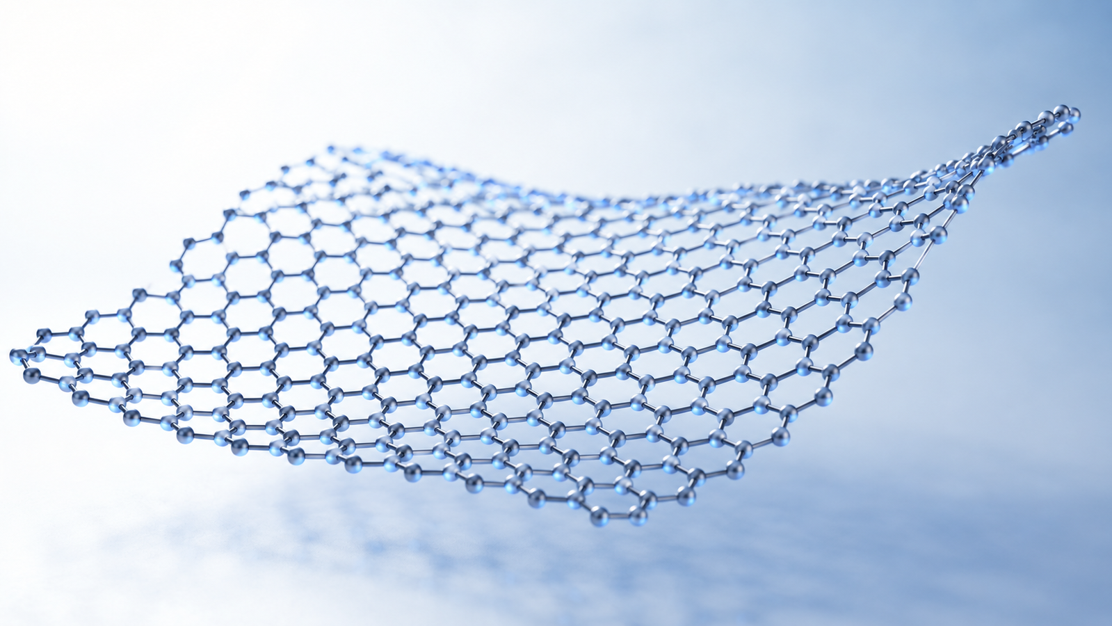
Graphene is a single layer of pure carbon atoms bonded together in a hexagonal lattice — the same pattern as a honeycomb. It is exactly one atom thick, roughly 0.335 nanometers, which makes it the thinnest material known and, for all practical purposes, the first truly two-dimensional material ever isolated.1 Stack many layers of graphene on top of one another and you get graphite, the soft gray carbon in an ordinary pencil. Graphene is simply that structure peeled down to a single sheet.
For decades, physicists believed a strictly two-dimensional crystal could not exist in isolation — thermal fluctuations were expected to make it unstable and cause it to crumple or melt. Graphene proved otherwise: the carbon-to-carbon bonds in the lattice are short (about 0.142 nm) and exceptionally strong, and the sheet stabilizes itself with gentle nanoscale ripples, remaining stable under ambient conditions.2 What makes graphene remarkable is not any single property but the combination: a material that is at once the thinnest, among the strongest, among the most conductive of both heat and electricity, nearly transparent, impermeable to gases, and flexible — all at the same time, in one substance.
How Graphene Was Discovered
Graphene was studied theoretically for over half a century before anyone held a piece of it. The breakthrough came in 2004 at the University of Manchester, where Andre Geim and Konstantin Novoselov were exploring whether a working transistor could be made from graphite. In a now-famous experiment, they used ordinary adhesive tape to peel progressively thinner flakes from a graphite crystal, transferred them onto a silicon wafer, and discovered that even single-atom-thick layers survived — and conducted electricity with a strong, controllable field effect.1 That simple "Scotch-tape method" finally delivered isolated graphene and revealed its electrons behaving as if they had no mass, moving as massless Dirac fermions.3
The discovery rewrote condensed-matter physics. Graphene's charge carriers travel through the lattice in a way described by the equations of relativistic quantum mechanics rather than ordinary electronics, a property that opened an entirely new field of research.4 In 2010, just six years after their experiments, Geim and Novoselov were awarded the Nobel Prize in Physics for isolating graphene and characterizing its properties. Since then, research into graphene and other two-dimensional materials has expanded explosively across physics, chemistry, materials science, and engineering.
Structure: The Honeycomb Lattice
Every property of graphene traces back to how its atoms are arranged. Each carbon atom in graphene is sp²-hybridized, forming three strong covalent σ bonds to its neighbors at 120-degree angles, all lying flat in the plane. That arrangement builds the characteristic hexagonal honeycomb. The fourth valence electron of each atom occupies a p-orbital sticking out of the plane; these combine into a vast delocalized π system spread across the entire sheet, and it is this sea of mobile electrons that carries graphene's remarkable electric current.
The in-plane σ bonds are what make graphene so stiff and strong — they resist stretching and compression fiercely — while the out-of-plane π electrons make it an excellent conductor. The two roles are cleanly separated, which is why graphene can be both mechanically extraordinary and electronically extraordinary without compromise.21 Explore the lattice yourself below: rotate it, inspect the bonds, and see how single sheets stack into graphite.
How Graphene Is Made
Turning graphene from a laboratory curiosity into an industrial material depends on how you make it, and there is no single best method — each trades off quality, size, and cost.
Mechanical exfoliation is the original Scotch-tape approach: peeling layers from graphite until single sheets remain. It produces the highest-quality, least-defective graphene, which is ideal for fundamental research, but only in tiny quantities — useless for mass production.1 Chemical vapor deposition (CVD) is the leading route to large-area films: a metal foil (usually copper, sometimes nickel or cobalt) is heated to 900–1000 °C inside a furnace, and a carbon-bearing gas such as methane is introduced, decomposing and reassembling into a graphene film on the metal surface, after which the chamber is cooled rapidly to prevent extra layers from forming.10 CVD made it possible to grow continuous graphene films large enough to be transferred roll-to-roll onto 30-inch transparent electrodes.11 The quality of CVD graphene depends sensitively on cooling rate, substrate purity, and gas composition, which is why controlling these variables is the central challenge of scaling it up.
Oxidation-reduction is the most scalable chemical route: graphite is oxidized to graphene oxide (GO), exfoliated in water, then chemically or thermally reduced back toward graphene as reduced graphene oxide (rGO). This path trades some electronic perfection for the ability to produce graphene-like material by the kilogram, in dispersions that can be coated, printed, and processed with ordinary solution chemistry — the foundation of graphene's use in composites, coatings, and energy storage.20 The persistent challenge across all methods remains producing large sheets of high, consistent quality efficiently enough for mass-market adoption.
The Properties That Make Graphene Extraordinary (With Real Numbers)
Graphene's reputation rests on a cluster of genuinely record-breaking measurements. Here are the real numbers, each from the primary literature — not the inflated figures that often circulate.
Strongest ever measured. By indenting free-standing single-layer graphene with an atomic-force microscope, researchers measured an intrinsic tensile strength of about 130 gigapascals (130 GPa) and a Young's modulus (stiffness) close to 1.0 TPa — establishing graphene, in the authors' own words, as the strongest material ever measured.5 For perspective, that strength is on the order of a hundred times that of structural steel for a sheet of the same thickness.
Thinnest and lightest. At one atom thick, graphene is the thinnest material that exists, yet remains visible to the naked eye. It is correspondingly light: a single square meter of graphene weighs only about 0.77 milligrams — roughly a thousand times lighter than the same area of paper.
Among the best conductors of electricity. Because each carbon contributes one mobile electron to a delocalized network, charge moves through graphene with extraordinarily little resistance. On a silicon-dioxide substrate at room temperature, electron mobility is already around 10,000–15,000 cm²/(V·s), but when graphene is suspended to remove the substrate's interference, mobility exceeds 200,000 cm²/(V·s) — far beyond silicon, and accompanied by an ambipolar field effect that lets the same sheet carry either electrons or holes.6 Theoretical and experimental work suggests the intrinsic mobility limit, set only by the lattice's own vibrations, is higher still.18 Graphene moves electrons faster, and with less energy lost, than the silicon in conventional chips.
Best conductor of heat. Graphene also conducts heat better than almost any known material. Optical measurements of suspended single-layer graphene at room temperature put its thermal conductivity in the range of roughly 4,840 to 5,300 W/(m·K)7 — higher than copper, diamond, or carbon nanotubes — which makes it a powerful candidate for drawing heat out of densely packed electronics.
Nearly transparent — by a fundamental constant. Despite stopping electrons so effectively, graphene barely stops light: a single sheet absorbs just 2.3% of visible light. Remarkably, that figure is not an accident of chemistry but is fixed by the fine-structure constant of physics, πα, independent of any material parameter.8 The combination of high transparency with high conductivity is exactly what makes graphene attractive as a replacement for brittle transparent electrodes.
Impermeable. A defect-free graphene sheet is so densely woven that not even helium, the smallest atom, can pass through it — graphene is the thinnest possible barrier membrane, standard atoms simply cannot fit between its carbon rings.9 Paradoxically, stacked graphene-oxide membranes built from this impermeable material let water through almost unimpeded while blocking nearly everything else, the basis of graphene-based filtration.15
Is Graphene Really Stronger Than Steel?
Yes — and the comparison is worth doing carefully, because it is the claim most often exaggerated. The honest version comes straight from the measurement: graphene's intrinsic strength is about 130 GPa.5 Structural steel, by comparison, has a tensile strength on the order of 0.4 to 2 GPa depending on grade. Compared like-for-like at the same thickness, graphene is roughly a hundred times stronger than steel — the often-quoted "200 times" figure refers to particular steel grades and assumptions, so a conservative "on the order of 100 times" is the defensible claim.
What makes this strength even more striking is that it comes with resilience, not brittleness in the everyday sense: graphene can stretch elastically by a remarkable margin — sustaining elastic strains far larger than ordinary crystals before it breaks — and springs back to its original dimensions.17 It combines the strength of a ceramic with a flexibility metals cannot match. The simulator below puts graphene's strength side by side with steel, Kevlar, and carbon nanotubes.
Graphene vs. Silicon vs. Copper
Graphene's promise is clearest when set against the materials it might one day supplement or replace. Against silicon, the backbone of modern electronics, graphene moves charge carriers more than an order of magnitude faster and stays conductive at atomic thinness where silicon's behavior degrades — though silicon has one feature graphene naturally lacks, an electronic band gap, which is why graphene does not simply replace silicon transistors but instead enables different devices.4 Against copper, the standard electrical and thermal conductor, graphene carries heat better and sustains enormous current densities in a far thinner, lighter form. The simulator below compares the three across the properties that matter most.
The takeaway is not that graphene wins on every axis — it is that no other single material is even in the conversation across so many axes at once. That breadth, rather than any one record, is what drives the research and investment behind it.24
What Graphene Is Used For
Graphene began as physics and is becoming engineering. Its applications fall into several broad families, and the simulator below lets you explore them interactively.
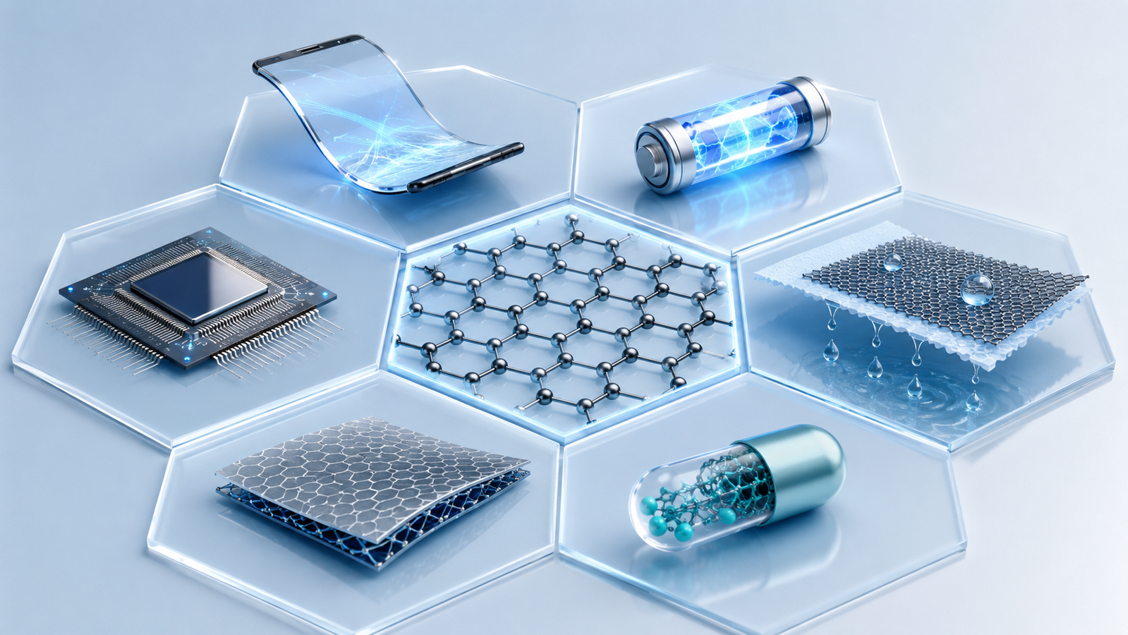
Electronics and optoelectronics. Graphene's blend of conductivity, transparency, and flexibility makes it a candidate to replace brittle, expensive indium tin oxide (ITO) in touchscreens, displays, and solar cells, and to enable flexible and foldable devices.19 Its optical properties also drive a wave of graphene photonics — ultrafast photodetectors, modulators, and mode-locked lasers.23 Energy storage. Its enormous surface area and conductivity make graphene and its derivatives strong electrode materials for supercapacitors and batteries, storing more charge and delivering it faster.12 Filtration and membranes. Graphene-oxide laminates sieve molecules and ions by size, with applications in water purification, desalination, and solvent separation.15 Sensors. Because adsorbing even a single gas molecule measurably changes graphene's resistance, it enables sensors of extreme sensitivity — down to individual molecules.13 Composites. Blended into polymers, metals, and concrete, small additions of graphene add strength, stiffness, and electrical conductivity for applications from aerospace to sporting goods.16 Biomedicine. Graphene oxide's large, functionalizable surface carries water-insoluble drugs into cells and supports imaging and biosensing.14 Comprehensive roadmaps lay out how these applications are expected to mature over the coming years.22
The Graphene Family: GO, rGO, and More
"Graphene" in commercial practice is really a family of related materials, and choosing the right one matters. Pristine monolayer graphene — a single defect-free sheet — delivers the textbook properties but is hardest and most expensive to make at scale. Few-layer graphene and graphene nanoplatelets stack a handful of layers, trading some peak performance for far easier processing and lower cost, and excel as conductive and reinforcing fillers. Graphene oxide (GO) is the oxidized, water-dispersible, electrically insulating form that is the workhorse precursor for solution processing. Reduced graphene oxide (rGO) restores much of graphene's conductivity from GO, giving an affordable, scalable, graphene-like conductor. Each sits at a different point on the trade-off between performance, processability, and cost — and a serious supplier offers the whole range, with the characterization data to tell them apart.25
Graphene Products from ACS Material
ACS Material has supplied graphene and related two-dimensional materials to researchers and industry since 2011, spanning the full family described above. For the foundational material, Single-Layer Graphene and the broader Graphene Series cover monolayer and few-layer powders and dispersions, while the CVD Graphene line provides continuous films on copper and transferred substrates for electronics and membrane work. The Graphene Oxide range — including single-layer GO powders and dispersions — serves solution processing and membranes, and Graphene Nanoplatelets address conductive and reinforcing filler applications. For energy researchers, the Battery Materials catalog applies these carbons to electrodes. Every lot ships with characterization data, and the applications team can help match the right grade — pristine, few-layer, oxide, or reduced — to your performance, processing, and budget requirements.
FAQ
What is graphene in simple terms?
Graphene is a single layer of carbon atoms arranged in a hexagonal honeycomb pattern, exactly one atom thick. It is the basic building block of graphite (pencil "lead"): a stack of millions of graphene sheets is graphite, and a single isolated sheet is graphene.
Is graphene stronger than steel?
Yes. Graphene's intrinsic strength is about 130 GPa, which is on the order of a hundred times stronger than structural steel of the same thickness, while being vastly lighter and also flexible. It is the strongest material ever measured.
Is graphene a good conductor of electricity?
Exceptionally. Electrons move through graphene faster than through silicon and with very little resistance — mobility exceeds 200,000 cm²/(V·s) in suspended, ideal-condition samples. Note this differs from graphene oxide (GO), which is an insulator until it is reduced.
How thick is graphene?
One atom — about 0.335 nanometers. That makes it the thinnest material known, and effectively two-dimensional. Despite this, a single sheet is strong enough to be free-standing and can even be seen with the naked eye.
Does graphene occur naturally?
Not as free isolated sheets. Graphene exists as the stacked layers inside graphite, which occurs naturally — the graphite in a pencil is made of countless graphene layers. Isolating a single layer requires processes like exfoliation, CVD, or chemical reduction.
Who discovered graphene and when?
Andre Geim and Konstantin Novoselov isolated graphene at the University of Manchester in 2004, using adhesive tape to peel single layers from graphite. They received the 2010 Nobel Prize in Physics for the work.
Why is graphene transparent if it conducts electricity?
Because it is only one atom thick, a graphene sheet absorbs just 2.3% of visible light — a value set by a fundamental physical constant. This rare combination of near-transparency and high conductivity is why graphene is pursued for transparent electrodes in touchscreens and solar cells.
What is graphene used for?
Major application areas include flexible and transparent electronics, energy storage (supercapacitors and batteries), water filtration and desalination membranes, ultra-sensitive sensors, lightweight high-strength composites, and biomedical drug delivery and imaging. Many uses are commercial today; others are still maturing from the lab.