
You have heard the headlines: graphene is stronger than steel, more conductive than copper, faster than silicon, and almost perfectly transparent. They are repeated so often that they have started to sound like marketing. So this guide does the unglamorous thing and puts the numbers next to each other — graphene measured against the very materials it is said to beat — with the primary research behind each figure and an honest account of where the comparison holds and where it quietly breaks down. If you want the broader picture of what graphene is and how it is made, our graphene facts overview covers the structure, discovery, and applications; here we focus on a single question: how does one atom-thick carbon actually compare?
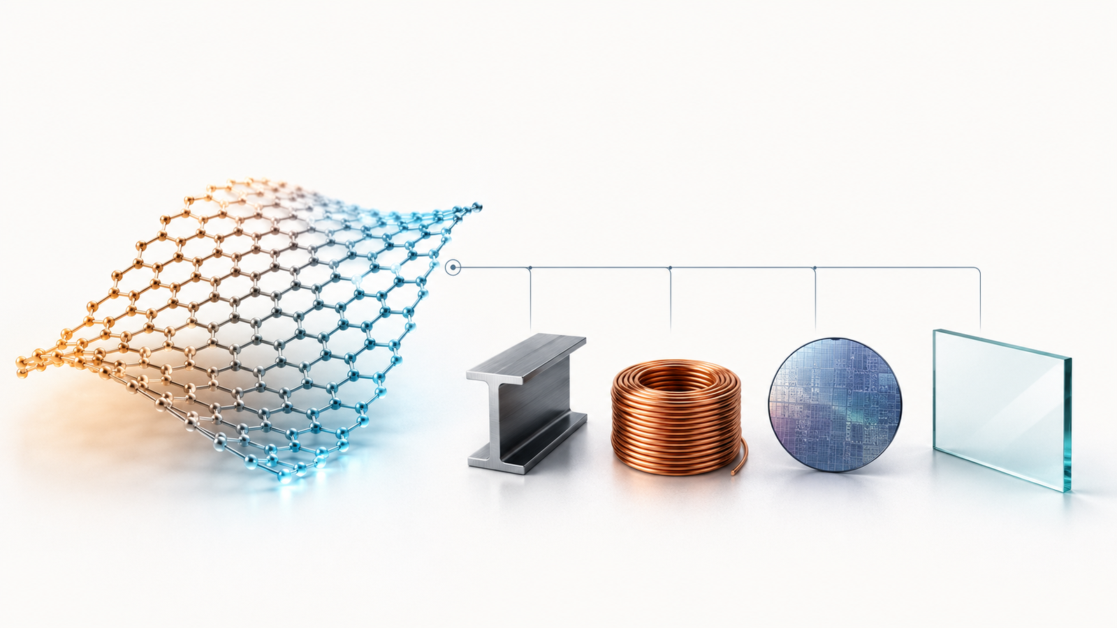
In one paragraph: on a per-property basis, defect-free single-layer graphene genuinely outperforms steel (about five times stiffer and tens of times stronger by intrinsic strength), copper (a similar resistivity but roughly a hundred times the current-carrying capacity), silicon (well over a hundred times the electron mobility — but with no band gap), and glass or ITO (about 97.7 % transparent per layer while still conducting). The catch is the phrase “defect-free single layer.” Those records are measured on tiny, pristine, suspended flakes; a real multilayer platelet, a CVD film, or a graphene composite falls well short, because defects, grain boundaries, layer count, and dispersion all dilute the ideal. The comparison below is therefore two stories at once: how extraordinary perfect graphene is, and why the material on a data sheet behaves differently.
What we are actually comparing
Graphene is a single sheet of carbon atoms locked into a hexagonal, honeycomb lattice, with carbon–carbon bonds about 0.142 nm long — the same strong, in-plane σ-bonded network that gives diamond and carbon fibre their stiffness, but arranged in one flat plane just one atom thick. It was first isolated and shown to be a stable two-dimensional crystal in 2004, work that earned the 2010 Nobel Prize in Physics1, and within a few years it had been crowned, with measurements rather than adjectives, the strongest, most conductive, and most thermally conductive material then known2. For the full story of its structure, discovery, and uses, see our complete guide to graphene; what matters for a fair comparison is one subtle point that the rest of this article keeps returning to.
Almost every record number for graphene is an intrinsic, single-layer, defect-free value — the property of one perfect sheet, often suspended so that no substrate interferes. That is the right thing to measure when you want to know what the material is, but it is not what arrives in a bottle. Commercial graphene is usually a powder of multilayer platelets, a transferred CVD film with grain boundaries, or a chemically derived oxide; each of those is further from the ideal sheet, and its numbers are lower. So when we say “graphene beats steel,” we mean a pristine monolayer beats steel in that specific property — a true and useful fact, and also one that has to be read carefully. With that caveat stated once, here is the head-to-head.
Strength & stiffness: graphene vs. steel
The famous claim is that graphene is “stronger than steel,” and the measurement behind it is unusually clean. By pressing an atomic-force-microscope tip into a free-standing monolayer membrane, Lee and co-workers extracted a Young’s modulus of E ≈ 1.0 TPa and an intrinsic breaking strength of σint ≈ 130 GPa for a defect-free sheet3. Put those beside steel, whose Young’s modulus is about 200 GPa and whose yield strength ranges from roughly 0.25 GPa for ordinary structural grades up to about 2 GPa for the strongest specialty alloys. Graphene is therefore about five times stiffer than steel and, at the intrinsic limit, tens to roughly a hundred times stronger.
The contrast is even sharper by weight. Graphene’s areal density is only about 0.77 mg m−2, so its specific strength — strength per unit mass — leaves steel far behind, which is exactly why it is so attractive for aerospace skins, composites, and anything where every gram counts. But the intrinsic 130 GPa is the strength of a perfect sheet; introduce a single vacancy, a grain boundary, or stack many layers into a platelet and the practical strength drops sharply. The honest framing is the one that survives scrutiny: graphene sets the ceiling for what a carbon membrane can do, and real reinforcement captures a useful fraction of it, not the headline figure. The simulator below compares an idealized graphene sheet against steel and other strong materials on a logarithmic strength chart, then switches to specific strength to show why graphene’s low weight widens the gap.
Conductivity & current: graphene vs. copper
This is the comparison most often garbled. Graphene is frequently said to be “a million times more conductive than copper,” which is simply wrong. Graphene’s in-plane electrical resistivity can reach roughly 1 µΩ·cm — comparable to, and in the cleanest samples slightly below, copper (about 1.7 µΩ·cm) and silver2. It is an outstanding conductor, but it is in the same league as the best metals, not a million times beyond them.
Where graphene genuinely pulls away is current-carrying capacity: how much current a conductor can sustain before it fails. A copper interconnect degrades by electromigration above roughly 106 A cm−2. Graphene nanoribbons have been driven to a breakdown current density on the order of 108 A cm−2 — about a hundred times higher — with Joule heating, not electromigration, as the eventual limit4. That combination of metal-class resistivity and far higher current density is what makes graphene compelling for on-chip interconnects and ultrathin conductors, where a copper line of the same cross-section would simply melt. The caveat returns here too: this is the behaviour of clean, narrow graphene, whereas large-area polycrystalline CVD film has a higher sheet resistance set by its grain boundaries and transfer quality. The model below contrasts the current a graphene and a copper conductor of equal cross-section can carry.
Mobility & the missing band gap: graphene vs. silicon
For electronics, the property that turns heads is carrier mobility — how quickly charge carriers move under a field. In the original 2004 devices, graphene already showed room-temperature mobilities around 10,000 cm2 V−1 s−11; suspending and current-cleaning a sheet to remove substrate scattering pushed that above 200,000 cm2 V−1 s−15. Silicon’s electron mobility is about 1,400 cm2 V−1 s−1. By this measure graphene is more than a hundred times faster, which is why it is so promising for high-frequency analog and radio-frequency devices.
And yet silicon still runs the world’s logic chips, for one decisive reason: graphene has no band gap. A digital transistor must switch fully off, and that requires a gap between the valence and conduction bands so the channel can be depleted of carriers. Silicon has a 1.1 eV gap; pristine graphene has none — its bands meet at a point, so a graphene field-effect transistor leaks current even in its “off” state and cannot give the high on/off ratio that digital logic needs. Researchers can open a small gap by cutting graphene into nanoribbons, stacking bilayers under a field, or straining it, but always at the cost of some mobility. The fair verdict is a split decision: graphene wins decisively on speed and mobility, silicon wins on switching, so the two are better seen as complementary than as rivals for the same socket.
Transparency: graphene vs. glass & ITO
That a sheet of metal-class conductor can also be nearly transparent is one of graphene’s strangest facts, and it has an exact explanation. The fraction of visible light a suspended monolayer absorbs is fixed by a fundamental constant — the fine-structure constant α — at πα ≈ 2.3 % per layer6. A single sheet therefore transmits about 97.7 % of light, two sheets about 95.4 %, and so on, with each added layer subtracting roughly another 2.3 points. Ordinary window glass transmits about 90 %, and indium tin oxide (ITO), the transparent conductor used in most touchscreens, around 85–90 % while being brittle and dependent on scarce indium.
The point is not that graphene is more transparent than glass — thick glass and a stack of graphene can land anywhere — but that graphene is transparent and conductive and flexible at once, the rare combination ITO delivers stiffly and graphene delivers on a bendable film. The trade-off is explicit and easy to model: more layers mean lower sheet resistance but lower transmittance, so a transparent-conductor designer picks a point on that curve. Drag the layer count below and watch transmittance fall in 2.3 % steps.
Heat: graphene vs. copper & diamond
Graphene is also among the best heat conductors ever measured. Using the temperature dependence of its Raman signal, Balandin and co-workers extracted a room-temperature thermal conductivity of roughly 4,800–5,300 W m−1 K−1 for suspended single-layer graphene7. Copper, the metal we reach for when we need to move heat, manages about 400 W m−1 K−1; even diamond, the benchmark solid conductor, is around 2,000. Graphene’s in-plane heat transport, carried efficiently by lattice vibrations in the stiff sp2 network, can therefore exceed both.
As everywhere else, the suspended single-layer figure is the ceiling. Place graphene on a substrate, stack it into few-layer flakes, or break it up with grain boundaries and the conductivity falls, because phonons now scatter off the substrate and the defects. Still, even reduced, graphene’s heat-spreading ability is what makes it attractive for thermal management in dense electronics — pulling heat sideways out of hot spots faster than a metal film of the same thickness could.
The numbers side by side
The table collects the headline properties for an ideal single layer of graphene against the materials it is usually compared with. Treat the graphene column as the intrinsic ceiling and the others as typical engineering values; each property carries a superscript link to the source of its graphene figure.
| Property | Graphene (ideal monolayer) | Steel | Copper | Silicon | Glass / ITO |
|---|---|---|---|---|---|
| Young’s modulus3 | ≈ 1,000 GPa (1 TPa) | ≈ 200 GPa | ≈ 120 GPa | ≈ 130 GPa | ≈ 70 GPa |
| Intrinsic tensile strength3 | ≈ 130 GPa | 0.25–2 GPa | ≈ 0.2 GPa | brittle | brittle |
| Electrical resistivity2 | ≈ 1 µΩ·cm | ≈ 20 µΩ·cm | ≈ 1.7 µΩ·cm | semiconductor | insulator |
| Current-carrying capacity4 | ≈ 108 A cm−2 | — | ≈ 106 A cm−2 | — | — |
| Electron mobility5 | > 200,000 cm2 V−1 s−1 | — | — | ≈ 1,400 cm2 V−1 s−1 | — |
| Band gap1 | 0 eV (gapless) | — | — | 1.1 eV | wide / — |
| Thermal conductivity7 | ≈ 5,000 W m−1 K−1 | ≈ 50 W m−1 K−1 | ≈ 400 W m−1 K−1 | ≈ 150 W m−1 K−1 | ≈ 1 W m−1 K−1 |
| Optical transmittance6 | ≈ 97.7% per layer | opaque | opaque | opaque | ≈ 90% (glass) |
The radar view below makes the shape of the comparison visible at a glance: each axis is one property, normalized so that “further out” is better, and you can toggle each material on or off. Graphene’s outline is conspicuously lopsided — enormous on mobility, current density, stiffness, and heat, and pointedly absent on band gap, which is the whole story of why it complements silicon rather than replacing it.
Ideal vs. real: why a data sheet differs
If you buy graphene and measure it, you will not see the numbers above — and that is expected, not a defect of the product. Every record in this article was measured on a small, pristine, usually suspended monolayer. Real materials depart from that ideal in four ways, each of which lowers performance: layer count (multilayer platelets behave partway between graphene and graphite), lateral size and grain boundaries (every edge and boundary scatters carriers and phonons and concentrates stress), defects and chemistry (vacancies and oxygen groups, as in graphene oxide, trade conductivity and strength for processability), and dispersion (in a composite, what matters is how well the platelets are separated and aligned, not the perfection of one sheet).
This is why a responsible specification talks about grade, not adjectives. Whether you need few-layer platelets for a conductive composite, a continuous CVD film for a transparent electrode, or a functional oxide for inks and membranes changes which fraction of the ideal you can realistically capture. The practical takeaway: use the figures here to understand the potential of the material and the direction each property moves, then consult the data sheet and our graphene properties overview for grade-specific behaviour before designing around a number.
Where graphene wins, where it doesn’t
Tallied honestly, the scorecard is clear and mixed. On a per-property, ideal-sheet basis, graphene wins decisively on specific strength and stiffness, electron mobility, current-carrying capacity, in-plane thermal conductivity, and the rare transparent-conductive-flexible combination. The incumbents still win where it matters commercially: silicon owns digital logic because it has a band gap; copper owns cheap bulk wiring because three-dimensional metal is inexpensive and mature; steel and engineering alloys own large structural parts because you cannot yet build a bridge from a monolayer; and glass and ITO remain entrenched by manufacturing scale. Graphene’s real near-term value is less “replace material X” than “add a property that X cannot provide” — conductivity to a polymer, heat-spreading to a chip, strength to a composite, flexibility to a transparent electrode. Read that way, the comparisons stop being a contest and become a map of where a one-atom-thick sheet is worth adding.
Graphene from ACS Material
ACS Material supplies graphene across the whole range discussed here, so you can match a grade to the property you actually need. Our graphene series spans single-layer graphene for work closest to the intrinsic limits, graphene nanoplatelets for conductive and structural composites, graphene dispersions for inks and coatings, and graphene oxide for chemistry, films, and membranes. For transparent-electrode and electronics work, our CVD graphene provides continuous films on copper and transferable substrates. For specifications, lateral size, layer number, and purity by grade, consult each product’s data sheet, and see the graphene facts guide for background on how these forms relate.
References
This article is provided by ACS Material LLC for educational purposes and compares graphene with conventional materials. The graphene figures cited — a Young’s modulus near 1 TPa and intrinsic strength near 130 GPa, an in-plane resistivity near 1 µΩ·cm and breakdown current density on the order of 108 A cm−2, suspended-sheet electron mobility above 200,000 cm2 V−1 s−1, thermal conductivity around 5,000 W m−1 K−1, and about 2.3 % optical absorption per layer — are intrinsic values measured on small, defect-free, usually suspended single-layer specimens in the referenced studies. A real multilayer platelet, a CVD film, graphene oxide, or any graphene composite will fall short of these figures, and actual performance depends on grade, layer number, lateral size, defect density, dispersion, and formulation; the values for steel, copper, silicon, glass, and ITO are typical engineering figures that vary with alloy, grade, and processing. Consult product datasheets and safety data sheets for grade-specific specifications and handling guidance. The interactive simulators are schematic teaching tools based on the stated relationships (a logarithmic tensile-strength comparison, current-carrying capacity, the πα per-layer transmittance law, and a normalized multi-property radar), not predictive design software; real measurements must be made and calibrated experimentally for each material and system.