-
Bilayer Graphene Gate Memcapacitor Array - Duke, 2025
May 21, 2026 | ACS MATERIAL LLCChen, J., Sarkar, A., Rahman, M. S., Ravel, V., Franklin, A. D., & Roy, T. (2025). Robust Memcapacitive Synapse Array for Energy-Efficient Motion Detection. *ACS Nano*. https://doi.org/10.1021/acsnano.5c02340
Duke University Pratt School of Engineering · ACS Nano · 2025
Duke University builds a 9x9 memcapacitor synapse array with a wet-transferred bilayer graphene gate, achieving 92.6% yield and picowatt motion sensing.
About this research
Researchers at Duke University Pratt School of Engineering used wet-transferred bilayer graphene (the same class of material distributed as ACS Material's Trivial Transfer Graphene) as the gate electrode of a high-yield memcapacitive synapse array that demonstrates short- and long-term plasticity and detects vehicle motion with only a few picowatts of power. The work, published in ACS Nano (2025) by Chen, Sarkar, Rahman, Ravel, Franklin, and Roy, shows that a metal-oxide-semiconductor (MOS) stack consisting of a graphene gate, 15 nm Al2O3, and 4 nm RF-sputtered indium-tin-oxide (ITO) can sustain 64 capacitance states, endure 2x10^4 electrical pulses, and process spatiotemporal motion frames directly inside the sensing pixel.
Motion detection in autonomous vehicles and edge AI is bottlenecked by the energy and latency cost of moving data between CMOS image sensors and processors; even idle image sensors consume 0.5-1.5 mW and exceed 150 mW in operation. Conductance-based memristive synapses help, but they leak static current and suffer from sneak paths in dense arrays. Capacitive memories are intrinsically leakage-free, yet prior memcapacitors used >1000 um^2 footprints, >5 V program voltages, and fewer than 16 states, undermining the case for monolithic 3D integration. A scalable, low-voltage, multi-bit memcapacitor with verified array statistics has been a missing piece of the neuromorphic hardware stack.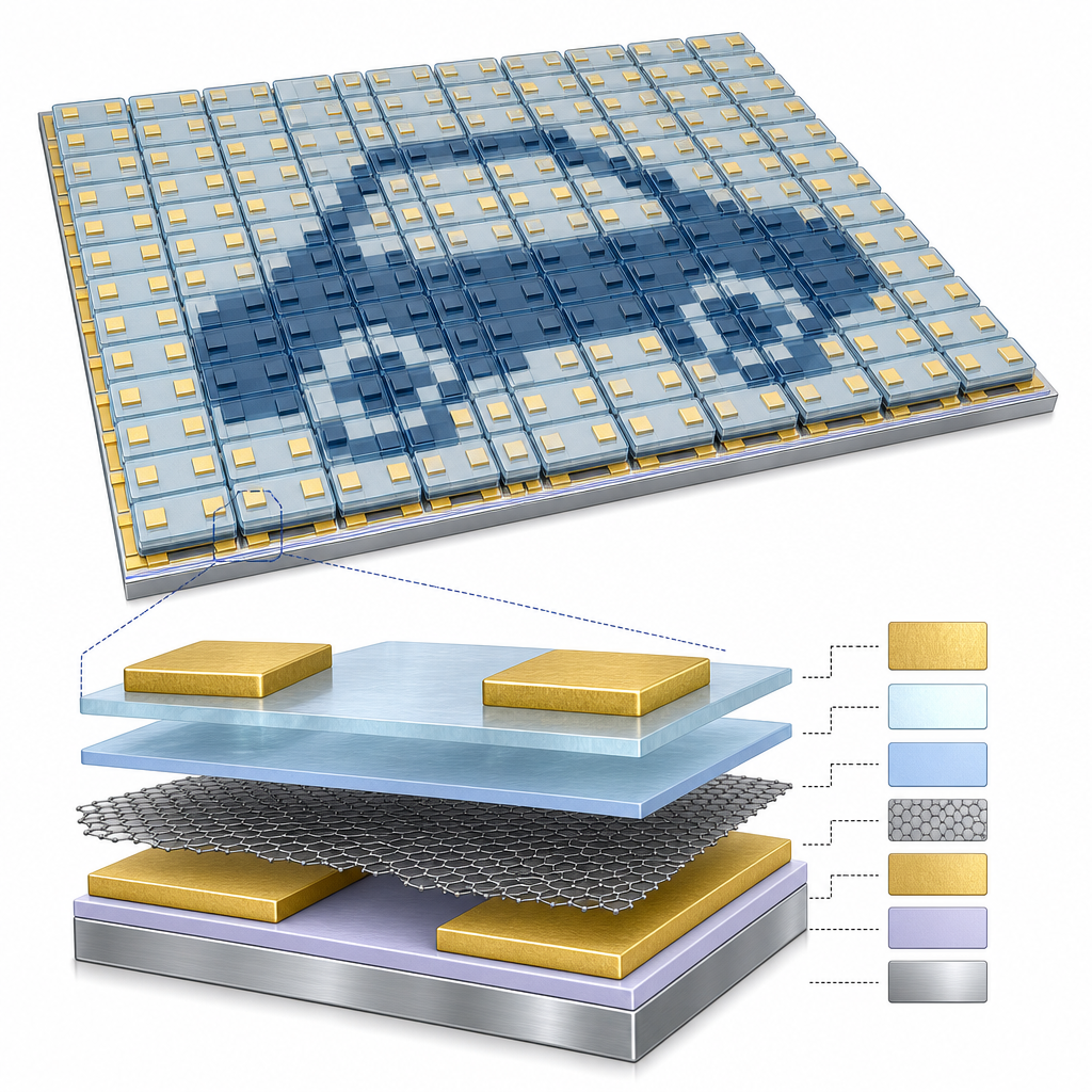
The ACS Material-relevant component is the bilayer graphene used as the top gate. The authors wet-transferred bilayer graphene onto Ti/Au (30/30 nm) contacts patterned on a thick 285 nm SiO2/Si substrate, then deposited 15 nm of Al2O3 by atomic layer deposition directly on the graphene, followed by 4 nm RF-sputtered ITO as the n-type channel and Ni/Au source-drain contacts. Graphene was chosen because it resists oxidation, can be scaled to atomic thickness, and adds negligible vertical parasitic capacitance to neighboring cells, an essential property at the 50 um^2 active area used here (10x smaller than previously reported memcapacitors). Al2O3 was selected for its strong adhesion and uniform ALD growth on the graphene surface, and ITO for back-end-of-line compatibility and high-yield deposition. The graphene/Al2O3 interface quality directly controls the density of interfacial trap states at the ITO/Al2O3 boundary, which in turn governs the hysteresis window that defines the memory effect.
The team fabricated a 9x9 array of 81 devices and characterized every cell. Seventy-five devices showed near-identical C-V hysteresis, yielding 92.6%. The high-capacitance state (HCS) and low-capacitance state (LCS), read at 1 V, gave an HCS/LCS ratio of 1.6 and a memory window of over 1.5 V under +/-4 V sweeps. Cycle-to-cycle uniformity was exceptional: LCS = 0.9 pF with sigma/mu = 1.1%, HCS = 1.21 pF with sigma/mu = 3.3% across 100 sweeps - far tighter than filamentary RRAM (>20%). Synaptic plasticity was tunable: negative pulses (-0.5 V to -2 V, 100-500 ms, 64-256 pulses) drove a continuous transition from short-term to long-term potentiation, while +1 V pulses produced symmetric depression with nonlinearity factors of 0.0204 (potentiation) and 0.0186 (depression). The array supported 64 nonoverlapping capacitance states (6-bit precision), >10^3 s retention, and stable bipolar cycling for 2x10^4 pulses. Power draw during motion sensing was in the picowatt range.
Leveraging short-term potentiation, the authors encoded car-motion trajectories as 4-bit binary pulse sequences and mapped each binary pixel onto an individual memcapacitor in the 9x9 grid. Four motion directions were reconstructed by reading the final capacitance pattern across the array, with measured frames matching the expected encoding. This in-sensor spatiotemporal processing eliminates pixel-to-processor data movement, which is the dominant energy cost in conventional CMOS image-sensor pipelines. The approach is directly relevant to event cameras, automotive perception, gesture recognition, and edge neuromorphic accelerators. Because the stack is BEOL-compatible, it is a candidate for monolithic 3D integration on top of CMOS logic, opening a path to dense, energy-frugal neuromorphic vision chips.
For researchers working on 2D-material-gated transistors, capacitive synapses, or graphene-Al2O3 interfaces, the quality and transferability of the graphene layer is decisive. ACS Material supplies Trivial Transfer Graphene and related CVD graphene products designed for clean wet-transfer onto arbitrary substrates, supporting workflows like the one demonstrated here. Groups exploring memcapacitive or thin-film MOS device platforms can source the bilayer-grade graphene gate material and matched CVD graphene films directly from the ACS Material catalog.How ACS Material products were used
- Trivial Transfer® Graphene (bilayer) (Trivial Transfer Series) — “The memcapacitive device features a wet-transferred bilayer graphene electrode on top of Ti/Au (30 nm/30 nm) gate contacts, with a 15 nm Al2O3 dielectric deposited by atomic layer deposition (ALD)”
Product Performance in this Study
The wet-transferred bilayer graphene served as the top gate electrode of the metal-oxide-semiconductor memcapacitor. Its sub-nanometer thickness minimized vertical parasitic capacitance from neighboring cells, while its oxidation resistance enabled uniform Al2O3 ALD deposition, supporting the 92.6% array yield.
Related product categories
Frequently asked questions
Why is wet-transferred bilayer graphene used as the gate electrode in this memcapacitor?
Bilayer graphene combines atomic-scale thickness with oxidation resistance and a smooth surface for ALD of Al2O3. At sub-nanometer thickness it contributes negligible vertical parasitic capacitance to neighboring cells in dense arrays, which is critical at the 50 um^2 cell size used here. Its inert surface also enables uniform, low-defect Al2O3 growth, which controls the interfacial trap density that gives rise to the memcapacitive hysteresis.
How does the 9x9 memcapacitor array achieve 92.6% yield and low device-to-device variation?
Yield comes from three engineering choices. RF-sputtered ITO deposits uniformly across the chip and is air-stable, avoiding channel degradation. ALD Al2O3 on graphene gives pinhole-free dielectric coverage. Wet-transferred bilayer graphene provides a reproducible, conductive top gate with no oxidation. Together they produce LCS sigma/mu of 1.1% and HCS sigma/mu of 3.3% over 100 cycles, with 75 of 81 devices working in the array.
What makes memcapacitors better than memristors for energy-efficient motion sensing?
Memcapacitors store information in a capacitance state rather than a conductance state, so they have no steady-state current and no leakage power when biased. This eliminates sneak-path currents in crossbar arrays and removes self-heating from high-density integration. In this work, motion sensing is performed with only a few picowatts of power, compared with hundreds of milliwatts for conventional CMOS image sensors during operation.