-
CVD Graphene Reveals Quasi-Ballistic Electrons — Kansas, 2023
May 22, 2026 | ACS MATERIAL LLCScott, R. J., Valencia-Acuna, P., & Zhao, H. (2023). Spatiotemporal observation of quasi-ballistic transport of electrons in graphene. *ACS Nano*. https://doi.org/10.1021/acsnano.3c08816
The University of Kansas · ACS Nano · 2023
University of Kansas researchers used ACS Material CVD and Trivial Transfer graphene to observe room-temperature quasi-ballistic electron transport at 22 km/s.
About this research
Researchers at The University of Kansas used CVD graphene supplied by ACS Material to construct a four-layer van der Waals heterostructure and directly observe room-temperature quasi-ballistic electron transport at 22 km s⁻¹. Published in ACS Nano in 2023, the work by Ryan J. Scott, Pavel Valencia-Acuña, and Hui Zhao places a MoS2/MoSe2 heterobilayer between two graphene monolayers and uses transient absorption microscopy to image how photogenerated electrons and holes spread in space and time. The graphene layers function as separate, independently addressable transport channels, and the experiment cleanly distinguishes classical diffusion in one layer from quasi-ballistic motion in the other.
Ballistic charge transport — where carriers move without scattering — is a long-standing goal in 2D-materials electronics because it sets the ultimate speed limit of devices such as terahertz transistors, photodetectors, and optoelectronic interconnects. Most experimental work on graphene transport relies on electrical contacts and patterned channels, which can mask intrinsic carrier dynamics. The Kansas team's all-optical approach bypasses contact resistance entirely: photoexcitation in the MoS2/MoSe2 type-II interface generates electron–hole pairs that subsequently transfer into the two graphene layers, where their motion is tracked optically. This addresses a broader open question in the van der Waals community: can heterostructure design produce free, independently moving charges rather than tightly bound interlayer excitons? The answer demonstrated here has direct implications for designing graphene/TMD optoelectronics.
ACS Material's CVD graphene played a central structural and electronic role in the device. According to the Methods section, "the bottom graphene layer is grown by ACS Material by chemical vapor deposition (CVD) and transferred on a 1-mm-thick quartz substrate." The MoS2 monolayer is then dry-stamped onto this bottom graphene using a PDMS transfer, followed by a MoSe2 monolayer. The top graphene layer is added using a different ACS Material product — Trivial Transfer CVD graphene supported by a 500-nm PMMA carrier film, which is floated on deionized water and laid over the assembled stack before the PMMA is dissolved with acetone. Between every transfer the sample is annealed in argon at 200 °C for at least five hours. The CVD-grown bottom film provides the high-mobility hole channel, while the Trivial Transfer top film hosts the quasi-ballistic electrons, making both ACS Material products integral to the four-layer device architecture.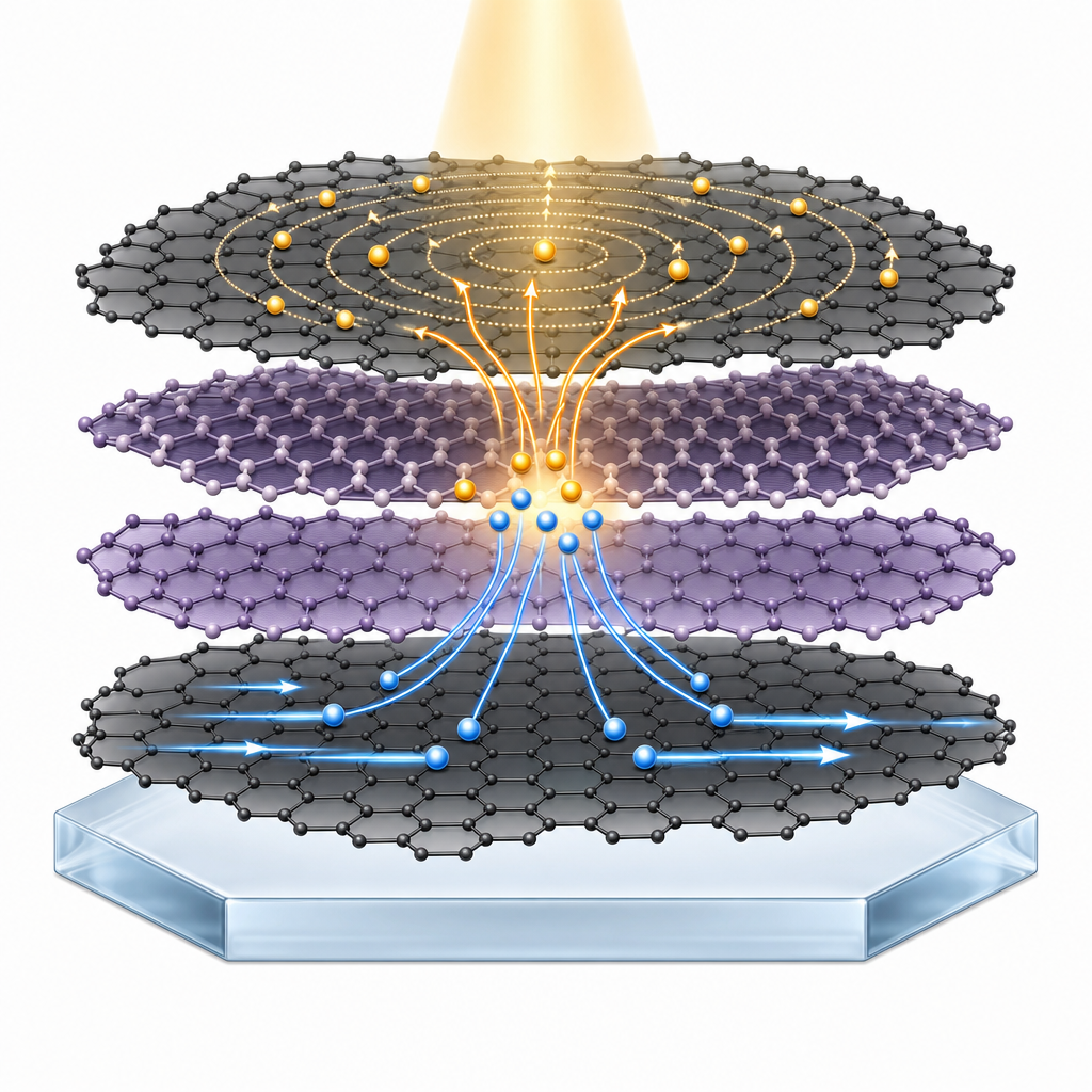
The transient absorption microscopy data deliver two clear and quantitative transport pictures. In the top graphene layer, holes spread by classical diffusion with a diffusion coefficient of 65 cm² s⁻¹, corresponding to a room-temperature charge mobility of 5000 cm² V⁻¹ s⁻¹ — values the authors note are characteristic of high-quality CVD graphene. In the bottom graphene layer, electrons behave fundamentally differently: their spatial profile expands linearly rather than diffusively over a 20-ps window, with a ballistic speed of 22 km s⁻¹. The authors verify that the signal originates from carriers inside the graphene rather than from excitons in the TMD layers by using two different probe energies (1.55 eV and 1.86 eV) tuned to the MoS2 and MoSe2 exciton resonances, exploiting the short-ranged dielectric screening that each graphene layer imposes on its adjacent TMD. Single-Gaussian fits to the spatial profiles further confirm that electrons and holes are not bound as interlayer excitons but propagate as independent free carriers, with markedly different dynamics in the two layers.
The immediate application area is high-speed graphene/TMD optoelectronics, including photodetectors, ultrafast modulators, and on-chip optical interconnects, where ballistic transport could remove conventional scattering-limited speed bottlenecks. The paper also points to a broader design principle: combining type-I and type-II band alignments in stacked 2D materials can be used to engineer carrier separation, suppress exciton binding, and route electrons and holes into distinct conduction channels. This has potential value for photovoltaics, exciton-blocking heterostructures, valleytronic devices, and quantum optoelectronic experiments that require contact-free generation of mobile carriers. The all-optical measurement methodology shown here can be transferred to other 2D-material stacks to benchmark their intrinsic transport behavior before device fabrication.
For researchers planning similar van der Waals experiments, the relevant materials — CVD Graphene on Copper Foil / Quartz and Trivial Transfer® Graphene — are available from ACS Material's graphene catalog. Both products are widely used for 2D-heterostructure fabrication because they provide monolayer coverage with the cleanliness needed for optical transport studies. The Kansas study demonstrates that this material grade is sufficient to resolve quasi-ballistic dynamics on picosecond timescales — a useful reference point when specifying graphene for ultrafast spectroscopy, photonic device prototyping, or layered 2D heterostructure research.How ACS Material products were used
- CVD Graphene (bottom layer transferred onto quartz substrate) (CVD Graphene) — “The bottom graphene layer is grown by ACS Material by chemical vapor deposition (CVD) and transferred on a 1-mm-thick quartz substrate.”
- Trivial Transfer® Graphene (top layer) (Trivial Transfer Series) — “The top graphene layer is placed over the sample using trivial transfer CVD graphene from ACS Material, which is covered in 500-nm thick polymethyl methacrylate (PMMA).”
Product Performance in this StudyThe ACS Material CVD graphene served as one of the two charge-transport layers in the van der Waals heterostructure, supporting hole diffusion with a measured diffusion coefficient of 65 cm² s⁻¹ and mobility of 5000 cm² V⁻¹ s⁻¹ — values consistent with high-quality CVD graphene.
Related product categories
Frequently asked questionsWhat is quasi-ballistic transport in graphene and why does it matter?
Quasi-ballistic transport means electrons move with minimal scattering, so their spatial spread grows linearly with time rather than as the square root of time as in classical diffusion. In this Kansas study the electrons moved at 22 km s⁻¹ for about 20 ps in CVD graphene. This regime sets the ultimate speed limit for graphene electronics and photodetectors and is highly desirable for ultrafast optoelectronic devices.
How is CVD graphene used in van der Waals heterostructure devices?
CVD graphene is grown on copper and transferred onto a target substrate such as quartz or SiO2/Si to provide a monolayer conducting sheet. In van der Waals stacks it is layered with transition metal dichalcogenides like MoS2 or MoSe2 using PDMS dry-transfer or wet PMMA-supported transfer. The graphene acts as a high-mobility charge channel, electrode, or screening layer, with carriers studied by optical or electrical means.
What is Trivial Transfer graphene and when is it preferred?
Trivial Transfer graphene is CVD graphene pre-attached to a polymer support film, designed for wet transfer onto arbitrary substrates. The film is floated on water, the target sample is brought up underneath, and the polymer is later dissolved. It is preferred when the underlying sample is fragile or already contains 2D layers — such as a finished MoS2/MoSe2 stack — that cannot tolerate the harsh chemistry of growth-substrate etching.