-
CVD Graphene–AgNW Hybrid Transparent Electrodes - Purdue, 2013
May 21, 2026 | ACS MATERIAL LLCChen, R., Das, S. R., Jeong, C., Khan, M. R., Janes, D. B., & Alam, M. A. (2013). Co-Percolating Graphene-Wrapped Silver Nanowire Network for High Performance, Highly Stable, Transparent Conducting Electrodes. *Advanced Functional Materials*. https://doi.org/10.1002/adfm.201300124
Advanced Functional Materials · 2013
Purdue University combines ACS Material CVD graphene on copper foil with silver nanowires to create co-percolating transparent electrodes reaching 13 Ω/sq at 88% transparency.
About this research
Researchers at Purdue University, publishing in Advanced Functional Materials (2013), demonstrated that combining commercial CVD single-layer graphene on copper foil from ACS Material with a silver nanowire (AgNW) network produces a co-percolating transparent conducting electrode (TCE) with sheet resistance as low as 22 Ω/sq at 88% optical transmittance, stabilizing to 13 Ω/sq after four months in ambient air. The work, led by Profs. David B. Janes and Muhammad A. Alam, shows that a 2D graphene film and a 1D AgNW network can each circumvent the other's transport bottleneck, yielding performance superior to standalone graphene, isolated AgNW networks, and conventional ITO references.
Transparent conducting electrodes are essential for photovoltaics, photodetectors, flat-panel displays, touchscreens, and image sensors. Indium tin oxide remains the industry standard but is brittle, costly, indium-supply-limited, and loses transparency above 1000 nm. Alternative materials each have a weakness: CVD single-layer graphene has 97% per-layer transparency yet suffers from high-resistance grain boundaries (HGBs) when grain sizes are small, while AgNW networks deliver high transparency but are dominated by large nanowire-nanowire junction resistances and contain micrometer-scale holes that hurt vertical current transport in stacked devices like LEDs and solar cells. The challenge addressed here is to drive sheet resistance below ~30 Ω/sq while preserving broadband transparency near 90% and mechanical flexibility — a regime where ITO has historically held the lead.
The Purdue team used commercial CVD graphene grown on copper foil from ACS Material (nominally single-layer graphene with an average grain size of approximately 1 μm). Using a standard PMMA-assisted wet transfer recipe, the graphene was transferred to 1 cm × 1 cm quartz substrates either before or after AgNW deposition, producing two hybrid configurations: Hybrid 1 (AgNWs deposited above the graphene) and Hybrid 2 (graphene transferred on top of the AgNW network). The AgNWs had an average diameter of ~90 nm, length of ~40 μm, and were deposited at four areal densities (2 × 10⁶ to 4.8 × 10⁶ cm⁻²), all well above the classical stick-percolation threshold of 3.6 × 10⁵ cm⁻². Raman spectroscopic mapping (D/G intensity ratio) and dark-field HRTEM confirmed the SLG nature, ~1 μm grain size, and ~600–800 nm overlapping grain regions of the as-transferred graphene.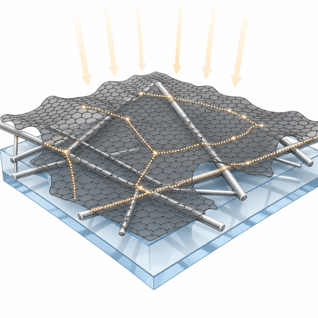
The as-received commercial graphene started at a baseline sheet resistance of ~770 Ω/sq after transfer, and the isolated AgNW networks alone exceeded 1 kΩ/sq due to poor wire-to-wire contact. Yet the Hybrid 2 architecture — graphene draped over the underlying nanowire network — delivered a measured sheet resistance of 22 Ω/sq at 88% transmittance at λ = 550 nm. Over four months of ambient storage, R_S dropped further and stabilized at 13 Ω/sq, the authors attributing this to junction healing rather than degradation. Hybrid 1 (nanowires on top of graphene) was substantially less effective because the wires did not make intimate contact with graphene or each other along their full length. The hybrid R_S is dramatically lower than the parallel combination of the two component resistances, confirming a genuine co-percolation effect: AgNWs bridge the HGBs in the graphene, while the conformal graphene sheet bridges the gaps between nanowires and reduces wire-to-wire contact resistance. Mechanical testing on flexible substrates showed stable resistance down to a bend radius of 8.3 mm, and the films retained their properties under applied mechanical pressure.
The immediate applications are clear: high-performance, ITO-free transparent electrodes for thin-film photovoltaics, OLEDs, flexible touch panels, photodetectors, and large-area image sensors. Because the conduction mechanism is generic, the co-percolation strategy can be extended to other 2D/1D combinations — for example, MoS₂ paired with carbon nanotubes — broadening the design space for low-cost, scalable transparent conductors. The combination of low sheet resistance, broadband transparency extending into the near-infrared (where ITO performs poorly), and mechanical robustness positions this approach for flexible and wearable optoelectronics, where ITO's brittleness is a recurring failure mode.
The finding has direct practical relevance for researchers exploring hybrid carbon/metal-nanowire electrodes. ACS Material supplies CVD graphene on copper foil and on a variety of receiver substrates, as well as silver nanowire dispersions and films, allowing groups to reproduce the co-percolating geometry without specialized growth infrastructure. The fact that low-cost, off-the-shelf commercial graphene — not high-purity laboratory-grown material — was sufficient to reach 13 Ω/sq at 88% transparency is a useful benchmark for procurement and process design in both academic labs and pilot-scale production.How ACS Material products were used
- CVD Graphene on Copper Foil (CVD Graphene) — “commercial CVD graphene grown on copper foil (nominally SLG and with an average grain size ≈ 1 μm, ACS Co., MA) was transferred onto a 1 cm × 1 cm quartz substrate”
Product Performance in this StudyThe commercial CVD single-layer graphene on copper foil, with an as-received sheet resistance of ~770 Ω/sq, served as the 2D component of the co-percolating hybrid transparent electrode. When combined with a AgNW network, the hybrid achieved sheet resistance as low as 22 Ω/sq (stabilizing to 13 Ω/sq) at 88% transparency, validating the graphene's role in bridging high-resistance grain boundaries of the network.
Related product categories
Frequently asked questionsHow does combining CVD graphene with silver nanowires lower sheet resistance?
The two materials form a co-percolating network. The silver nanowires bridge the high-resistance grain boundaries that limit conduction in CVD single-layer graphene, while the graphene sheet bridges the gaps and high-resistance contacts between nanowires. This mutual circumvention drives the hybrid sheet resistance well below the parallel combination of the two components, reaching 22 Ω/sq at 88% transmittance versus 770 Ω/sq for graphene alone.
Why is the graphene-on-top (Hybrid 2) configuration better than nanowires-on-top?
When the silver nanowire network is deposited first and CVD graphene is transferred on top, the conformal graphene film presses against the nanowires and pulls them into intimate contact with each other and with the substrate. This dramatically reduces nanowire-nanowire junction resistance and improves graphene-nanowire coupling. The inverted Hybrid 1 geometry leaves wires only sparsely touching the underlying graphene, producing much higher sheet resistance.
Is commercial CVD graphene on copper foil good enough for transparent electrodes?
Yes. The Purdue team used unmodified commercial CVD graphene on copper foil with a roughly 1 μm grain size and a starting sheet resistance of 770 Ω/sq. After integration with a silver nanowire network, the hybrid film reached 13 Ω/sq at 88% transparency without any additional doping, purification, or layer stacking, showing that low-cost off-the-shelf graphene is sufficient for high-performance ITO-replacement electrodes.