-
Silver Nanowire Electrodes for CIGS Solar Cells - Hanbat National University, 2018
May 21, 2026 | ACS MATERIAL LLCLee, S., Lee, J. S., Jang, J., Hong, K., Lee, D., Song, S., Kim, K., Eo, Y., Yun, J. H., Gwak, J., & Chung, C. (2018). Robust nanoscale contact of silver nanowire electrodes to semiconductors to achieve high performance chalcogenide thin film solar cells. *Nano Energy*. https://doi.org/10.1016/j.nanoen.2018.09.027
Nano Energy · 2018
Researchers used ACS Material AgNW-L30 silver nanowires as transparent top electrodes in CIGS thin-film solar cells, achieving robust nanoscale contact and high efficiency.
About this research
Researchers led by Choong-Heui Chung at Hanbat National University demonstrated that silver nanowires supplied as ACS Material AgNW-L30 can replace sputtered transparent conductive oxides in high-performance Cu(In,Ga)Se2 (CIGS) chalcogenide thin-film solar cells, achieving efficiencies competitive with the conventional i-ZnO/ZnO:Al window layer. Published in Nano Energy in 2018, the paper introduces a process that embeds AgNWs at the CdS/CIGS junction using a second chemical bath deposition step, producing a robust nanoscale electrical contact between the metallic nanowires and the underlying semiconductor. The result is a flexible, vacuum-free transparent electrode architecture suitable for next-generation chalcogenide photovoltaics.
Transparent conductors are a cost and process bottleneck for thin-film solar cells. Sputtered transparent conductive oxides such as ZnO:Al require vacuum equipment, high-temperature processing, and brittle ceramic layers that are incompatible with flexible substrates. Silver nanowire networks have long been proposed as an alternative because they combine high optical transmittance with low sheet resistance and can be solution-processed at low temperature. However, integrating AgNW networks directly onto semiconductors like CdS/CIGS has been hindered by poor mechanical adhesion, weak electrical coupling at the nanoscale wire–semiconductor interface, and parasitic recombination losses. Solving these contact problems is critical for chalcogenide, CZTS, and perovskite tandem architectures where solution-processed top electrodes would dramatically simplify manufacturing and enable flexible photovoltaic modules.
The ACS Material AgNW-L30 product was the central component of the new transparent electrode. The Methods section reports that the AgNWs were dispersed in ethanol and that the nanowires had diameters of approximately 30 nm and lengths of 100–200 µm, geometric parameters well suited for percolative conductive networks. The dispersion was spin-coated onto CdS-coated CIGS absorbers and annealed at 120 °C for 5 minutes to remove solvent and form an initial conductive mesh. Critically, a second CdS layer was then grown over the AgNW network by chemical bath deposition, with a growth rate of about 3 nm/min after a 6–7 minute incubation period. This overcoating physically embedded the wires into the semiconductor surface, producing intimate nanoscale contact regions that the authors describe as the key enabler of robust electrical coupling. Measured electrode performance was 90–95% transmittance and 15–30 ohm/sq sheet resistance, comparable to commercial ITO.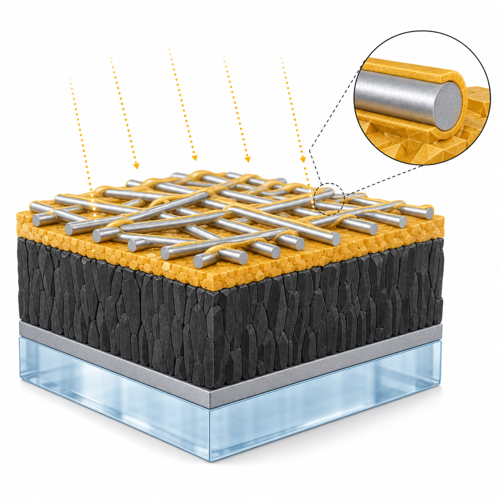
The completed CIGS devices used the architecture transparent electrode/CdS/CIGS/Mo/Glass, with 2 µm CIGS absorbers co-evaporated onto Mo-coated soda-lime glass and 75 nm primary CdS buffers. The authors benchmarked their AgNW-based devices against standard cells with sputtered i-ZnO/ZnO:Al window layers (500 nm). Current–voltage characteristics were measured under AM1.5G white light at 1000 W/m² as well as under red-light illumination filtered through a 525 nm long-pass filter to probe spatial collection uniformity. Device morphology and the buried contact were verified by SEM and cross-section TEM, which confirmed that the second CdS layer conformally wrapped the embedded AgNWs and bridged the wire–CdS junction at the nanoscale. The combination of high transmittance, low sheet resistance, and reduced contact resistance produced solar cells with performance rivaling the sputtered ZnO:Al control, while eliminating vacuum sputtering of the window layer entirely. The strategy also offers a path toward lower processing temperatures and improved mechanical compliance for flexible substrates.
The demonstrated approach is directly relevant to CIGS, CdTe, CZTS, and emerging perovskite/chalcogenide tandem photovoltaics, where solution-processed top electrodes can reduce module cost and enable roll-to-roll fabrication. Beyond solar cells, the AgNW-embedded-in-semiconductor concept is applicable to transparent electrodes for thin-film photodetectors, transparent thin-film transistors, and flexible optoelectronics where electrode–semiconductor contact resistance limits device performance. The authors note that the chemical-bath embedding strategy is generalizable to other chalcogenide and oxide semiconductors that can be grown from solution at low temperatures, opening a route to vacuum-free transparent electrode integration across the photovoltaic and display industries.
Researchers building transparent electrodes, flexible solar cells, or other AgNW-based devices can source the same long, thin silver nanowires used in this study from ACS Material's Nanowire Series, which includes silver nanowires with diameters and lengths comparable to the AgNW-L30 grade reported here. The reproducibility of the percolation network and the reliability of the embedded contact depend strongly on nanowire dimensions and dispersion quality, both of which are specified by the supplier. For groups working on chalcogenide photovoltaics, perovskite tandems, or transparent conductive coatings, this paper provides a concrete protocol and a clear benchmark for what consistent, well-characterized silver nanowires can deliver in real device contexts.How ACS Material products were used
- Silver Nanowire (AgNW-L30) (Nanowire Series) — “AgNWs (ACS Material, Agnw-L30) were dispersed in ethanol, and their diameter and length were approximately 30 nm and 100~200 µm, respectively. AgNW electrodes give a typical T of 90~95% and an Rs of 15~30 ohm/sq”
Product Performance in this StudyThe ACS Material AgNW-L30 silver nanowires functioned as the transparent top electrode in CIGS thin-film solar cells, delivering 90–95% transmittance and 15–30 ohm/sq sheet resistance. After embedding via a second CdS chemical bath deposition, the AgNW electrodes enabled robust nanoscale contact and high device efficiency comparable to standard sputtered ZnO:Al window layers.
Related product categories
Frequently asked questionsHow does embedding silver nanowires in CdS improve solar cell contact?
Spin-coating AgNWs onto a CdS/CIGS surface alone leaves the wires resting on top with weak mechanical and electrical contact. By growing a second CdS layer via chemical bath deposition at about 3 nm/min, the new CdS conformally wraps each nanowire and physically embeds it into the semiconductor. This creates a robust nanoscale junction that lowers contact resistance and reduces recombination at the wire–semiconductor interface.
What are the optical and electrical properties of AgNW transparent electrodes for solar cells?
The AgNW electrodes used in this CIGS study delivered 90–95% optical transmittance across the visible range and a sheet resistance of 15–30 ohm/sq. These values are comparable to commercial indium tin oxide while allowing solution-based, low-temperature processing. The nanowires were approximately 30 nm in diameter and 100–200 µm long, dimensions that promote a high-aspect-ratio percolation network with low optical scattering.
Why is AgNW length and diameter important for transparent electrode performance?
Long, thin silver nanowires form percolating conductive networks at lower areal densities, which preserves optical transmittance while minimizing sheet resistance. The 30 nm diameter, 100–200 µm length nanowires in this study reach the percolation threshold with relatively few junctions, reducing both optical haze and total junction resistance. Shorter or thicker wires would require higher loadings, degrading transmittance and increasing scattering losses.