-
CVD Bilayer Graphene for Flexible Si Solar Cells - UCF, 2019
May 26, 2026 | ACS MATERIAL LLCDas, S. et al. (2019). A leaf-inspired photon management scheme using optically tuned bilayer nanoparticles for ultra-thin and highly efficient photovoltaic devices. *Nano Energy*. https://doi.org/10.1016/j.nanoen.2018.12.072
Nano Energy · 2019
University of Central Florida used ACS Material CVD bilayer graphene on copper foil to build leaf-inspired flexible graphene/Si solar cells reaching 8.8% efficiency.
About this research
Researchers at the University of Central Florida, together with collaborators at KAUST, used CVD bilayer graphene on copper foil purchased from ACS Material to build an ultrathin, flexible graphene/silicon Schottky junction solar cell that reached 8.8% power conversion efficiency with a leaf-inspired bilayer nanoparticle light-trapping scheme. The work, published in Nano Energy in 2019, achieves the highest reported watt-per-gram silicon utilization (1.89) among graphene/Si solar cells while keeping the silicon absorber only 20 μm thick. The design decouples optical and electrical loss mechanisms by avoiding any structuring of the Si surface.
Ultrathin crystalline silicon photovoltaics are central to the move toward bendable, roll-to-roll-processable solar modules, but planar Si reflects a large fraction of the AM1.5G spectrum and conventional surface texturing increases recombination losses. Borrowing from how leaves capture, focus, and scatter light through layered cellular structures, the authors propose an all-dielectric bilayer of spheroidal silica and titania nanoparticles on top of a transparent graphene electrode. The challenge for the graphene layer is to combine high optical transmittance with low sheet resistance and to form a robust Schottky junction with n-Si, which is where the choice of CVD bilayer graphene becomes critical.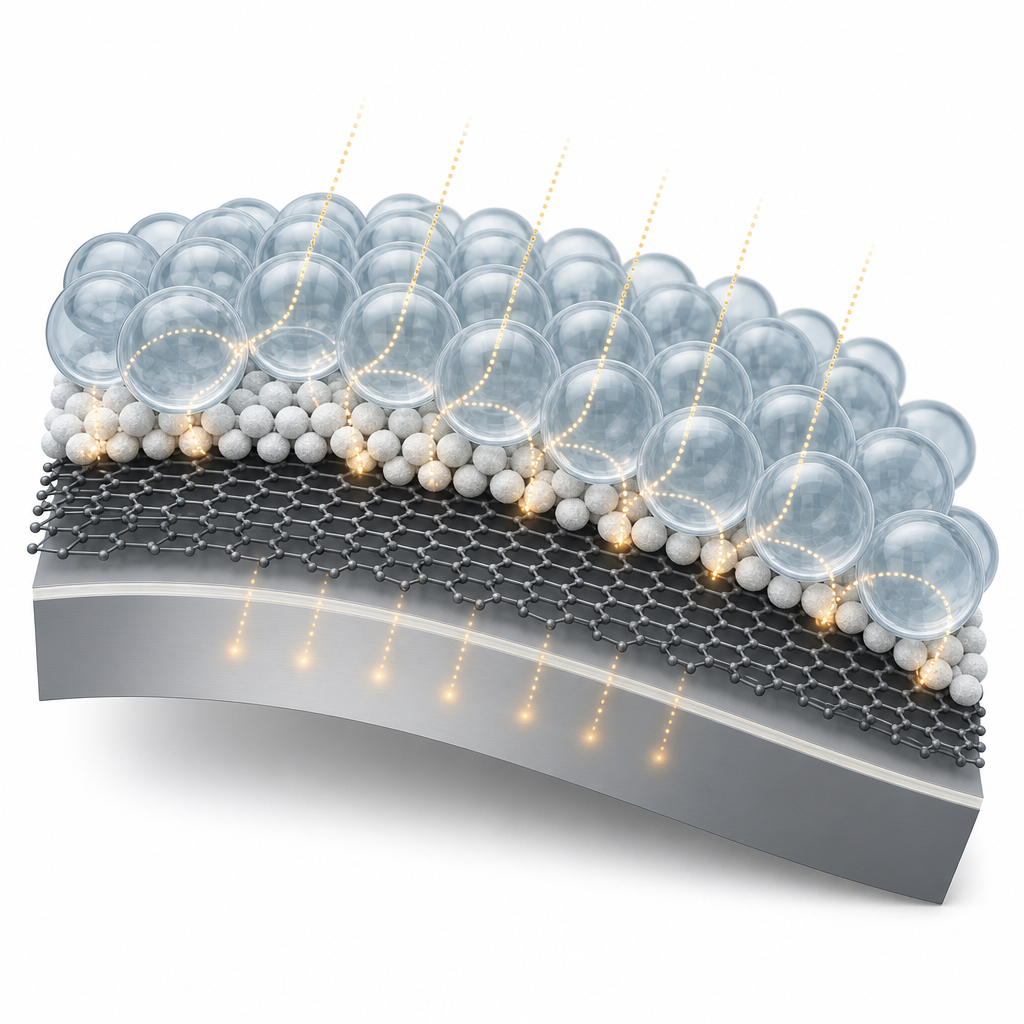
The bilayer graphene was grown on copper foil and acquired from ACS Material. After defining contacts on a 20 ± 2 μm thick n-Si <100> substrate passivated by 1 nm of atomic-layer-deposited Al2O3, the team p-doped the as-grown graphene by spin-casting 20 mM AuCl3 in nitromethane. Titania and then silica nanoparticles were spin-coated onto the doped graphene/Cu foil to form a hexagonal close-packed bilayer (titania d ≈ 120 nm beneath silica D ≈ 610 nm, D:d ≈ 6:1). The composite stack was then transferred onto the silicon substrate by a PMMA-assisted wet transfer, and the device was annealed in a 1:9 H2:N2 mixture at 400 °C for 3 hours. Bilayer graphene was chosen because its sheet resistance is roughly half that of monolayer graphene at the cost of only a small drop in transmittance (95.3% vs. 97.6%), giving a favorable trade-off for the transparent electrode of a Schottky solar cell.
FDTD simulations identified a D = 600 nm / d = 100 nm silica/titania bilayer on a 20 μm thick Si substrate as the optimum, predicting an integrated reflectance of about 7.32%. Experimentally, the fabricated device showed broadband reflectance of 10.3% over 400-1100 nm, an ~80% reduction relative to bare graphene/Si of the same thickness, with reflectance below 3% in the 540-740 nm window. The graphene/Si solar cell without nanoparticles delivered 6.8% efficiency with Jsc = 22.8 mA/cm², Voc = 0.49 V, and FF = 61%. Adding the leaf-inspired light-trapping coating raised the efficiency to 8.8% (a 30% relative gain), Jsc to 28 mA/cm² (matched by EQE integration at 26.8 mA/cm²), with Voc improving slightly to 0.51 V and no change in fill factor, series resistance, or shunt resistance. EQE rose by about 30% across the spectrum due to whispering gallery mode coupling in the silica spheres followed by forward scattering through the titania layer into the Si. The omnidirectional response was confirmed by less than 14% increase in integrated reflectance up to 50° incidence, and the laminated flexible device retained its J-V characteristics over more than 10³ bending cycles at bend radii of 20, 10, and even 3 mm.
The approach is directly relevant to flexible photovoltaics, roll-to-roll Si module manufacturing, building-integrated solar, and any thin-film cell technology that needs broadband, polarization-independent, omnidirectional anti-reflection without active-layer texturing. Because the silica/titania bilayer is purely dielectric and lossless, the same concept could be extended to perovskite, CIGS, or amorphous Si platforms where surface recombination is a concern. The authors also point to graphene-based Schottky junctions as a viable low-cost route within the monocrystalline Si solar cell roadmap.
For researchers working on graphene/Si Schottky devices, transparent electrodes for photovoltaics, or 2D-material-based optoelectronics, the CVD bilayer graphene on copper foil supplied by ACS Material provided the combination of optical transmittance, sheet resistance, and transferability needed to realize the bendable cell. The same CVD graphene on copper foil product is available through ACS Material for groups pursuing similar Schottky solar cell, photodetector, or transparent conductor research.How ACS Material products were used
- CVD Graphene on Copper Foil (bilayer) (CVD Graphene) — “Bilayer graphene grown on copper foil (purchased from ACS Materials Inc.) was transferred onto the Si substrate by polymethyl methacrylate (PMMA) assisted wet transfer process.”
Product Performance in this StudyThe bilayer CVD graphene from ACS Material served as the transparent conducting electrode and Schottky junction partner with Si. After AuCl3 p-doping and integration with the bilayer nanoparticle light-trapping scheme, the device reached 8.8% power conversion efficiency, a 30% relative improvement over the bare graphene/Si cell.
Related product categories
Frequently asked questionsWhy use bilayer CVD graphene instead of monolayer for graphene/Si Schottky solar cells?
Bilayer CVD graphene has approximately half the sheet resistance of monolayer graphene while reducing optical transmittance only slightly, from 97.6% to 95.3%. For a Schottky-junction solar cell where the graphene serves simultaneously as the transparent window and the current-collecting electrode, this trade-off gives a net improvement in fill factor and series resistance and supports higher short-circuit current density.
How does a silica/titania bilayer nanoparticle coating improve thin silicon solar cell efficiency?
The larger silica spheres on top sustain whispering gallery modes that focus and waveguide incoming light, while the smaller titania spheres underneath act as forward-scattering leaky channels that funnel light into the silicon absorber. On a 20 μm thick Si cell this dropped broadband reflectance to 10.3%, raised Jsc from 22.8 to 28 mA/cm², and lifted power conversion efficiency from 6.8% to 8.8%.
What role does AuCl3 doping play in CVD graphene transparent electrodes?
Spin-casting 20 mM AuCl3 in nitromethane p-dopes CVD graphene, raising its work function so that the graphene/Si Schottky barrier height increases. This improves open-circuit voltage and lowers the sheet resistance of the graphene electrode, which in turn improves the fill factor of the solar cell without compromising the optical transmittance needed for the transparent window layer.