-
CVD Graphene 3D Tubular Photodetectors - Beijing Jiaotong University, 2019
Jun 12, 2026 | ACS MATERIAL LLCDeng, T. et al. (2019). Three-dimensional graphene field-effect transistors as high-performance photodetectors. *Nano Letters*. https://doi.org/10.1021/acs.nanolett.8b04099
Beijing Jiaotong University · Nano Letters · 2019
Beijing Jiaotong University researchers built self-rolled 3D graphene FET photodetectors from CVD graphene by ACS Material, reaching >1 A/W from UV to THz.
About this research
Researchers at Beijing Jiaotong University, working with collaborators at Tsinghua University and the Institute of Microelectronics of the Chinese Academy of Sciences, used monolayer CVD graphene supplied by ACS Material, LLC to fabricate self-rolled-up three-dimensional (3D) graphene field-effect transistor (GFET) photodetectors that operate from the ultraviolet through the terahertz. By rolling a planar buried-gate GFET into a multi-winding microtube, the team achieved photoresponsivities above 1 A/W in the UV and visible and 0.232 A/W at 3.11 THz, with an electrical bandwidth of about 1.38 MHz at room temperature. The paper, published in Nano Letters, demonstrates that geometric engineering of CVD graphene can simultaneously deliver high responsivity, broad spectral coverage, and high speed in a single device.
Photodetectors based on conventional planar GFETs have long been limited by the 2.3% optical absorption of single-layer graphene, capping responsivity at a few mA/W. Hybrid approaches that pair graphene with quantum dots or other absorbers can lift responsivity by many orders of magnitude but only at the cost of slow response times. Plasmonic and Fabry-Perot enhancement schemes work at narrow design wavelengths. A device architecture that simultaneously enhances absorption, preserves graphene's intrinsic ultrafast carrier dynamics, and remains broadband would be valuable for imaging, optical communications, terahertz spectroscopy, and sensing. The 3D tubular GFET demonstrated here directly targets this gap by using a self-rolled-up dielectric stack to form a natural resonant microcavity around the graphene channel.
The ACS Material CVD graphene was used as the active channel of the GFET. After sputtering a 50 nm Al sacrificial layer on Si, the authors deposited compressively and tensile strained SiNx layers by PECVD, patterned a Cr/Au gate, and deposited a 30 nm SiO2 gate dielectric. Monolayer CVD graphene from ACS Material was then transferred onto the SiO2 surface and patterned by oxygen plasma etching to form a 30 μm × 400 μm conductive channel, followed by evaporation of Cr/Au source and drain electrodes. Selective etching of the Al sacrificial layer in FeCl3 released the strained SiNx stack, which rolled the planar GFET into a microtube. By tuning the SiNx thicknesses and device dimensions, the authors produced 3D GFETs with diameters from 30 to 65 μm and winding numbers from one to five. Raman spectroscopy confirmed that the graphene survived the roll-up process intact.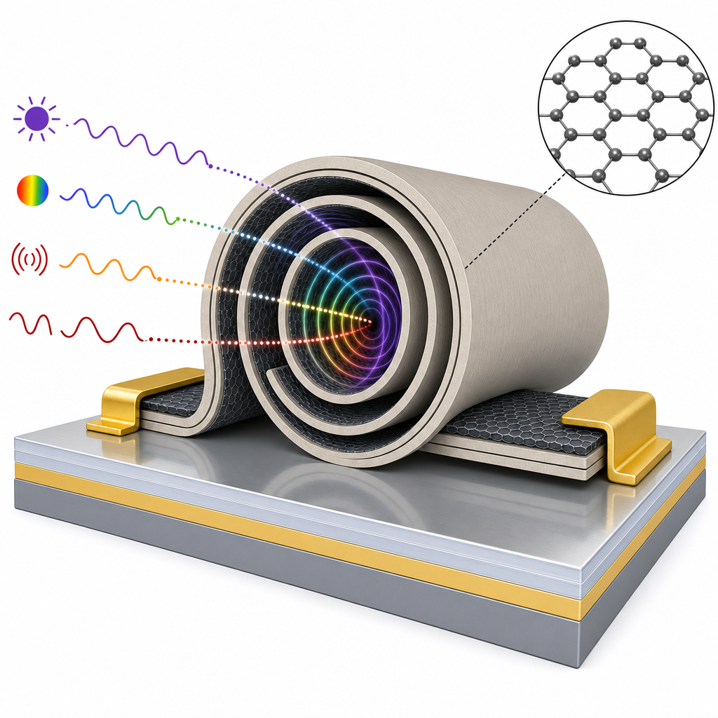
The rolled 3D GFETs retained typical ambipolar transfer characteristics. The 2D reference device showed a Dirac point of 6 V and a hole mobility of 1070 cm²/(V·s) with a metal-graphene contact resistance of 676 Ω; after rolling, the Dirac point shifted to 7 V, mobility dropped to 780 cm²/(V·s), and contact resistance rose to 804 Ω. Under 325 nm illumination at zero gate and source-drain bias, a two-winding 3D GFET delivered a responsivity of 2.3 mA/W—three orders of magnitude higher than the 1.6 μA/W from the planar reference. Gate biasing pushed the responsivity above 1 A/W, roughly two orders of magnitude higher than typical back-gated 2D GFET photodetectors. Five-winding 3D GFETs reached 113.2 mA/W at 119 μm (2.52 THz), 232.8 mA/W at 96 μm (3.11 THz), and 16.4 mA/W at 10.6 μm. The estimated noise-equivalent power at 3.11 THz was approximately 48 pW/Hz^(1/2) and the specific detectivity was 2.8 × 10^10 Jones. Pulsed laser measurements at 633 nm gave rise and fall times of 265 ns and 220 ns and a 3 dB electrical bandwidth of 1.38 MHz. Finite element simulations attributed the gains to a tubular optical microcavity that locally enhances the field by roughly 500× and an enlarged graphene-light interaction area.
The 3D GFET architecture is relevant to terahertz imaging, mid-infrared sensing, polarization-resolved detection, optical communications, and on-chip photonic readout, since it covers UV to THz wavelengths within one device platform. The 5×3 microtube array shown in the paper indicates that the fabrication is compatible with large-scale, parallel device integration. The authors note that replacing single-layer with stacked multilayer graphene, improving the asymmetry of source-drain electrodes, and optimizing tube diameter could further push responsivity, bandwidth, and detectivity. The same self-rolled-up process can in principle be extended to MoS2, black phosphorus, and other 2D materials to create 3D versions of their optoelectronic devices.
For researchers building graphene-based optoelectronic devices, the work shows that the quality of commercial monolayer CVD graphene is sufficient to enable advanced geometries such as multi-winding microtubes without sacrificing carrier mobility or optical performance. ACS Material's CVD graphene on copper foil, used in this study, is available to groups working on photodetectors, terahertz electronics, and flexible optoelectronics who need a reproducible monolayer starting material compatible with transfer onto SiO2, SiNx, and similar dielectric stacks. Reliable supply of monolayer graphene supports the device-level innovations that connect 2D materials research to practical photodetection systems.How ACS Material products were used
- CVD Graphene on Copper Foil (CVD Graphene) — “monolayer CVD-grown graphene (ACS Material, LLC) was transferred onto the SiO2 layer and patterned using oxygen plasma etching”
Product Performance in this StudyThe monolayer CVD graphene from ACS Material served as the conductive channel of the rolled-up 3D GFET photodetectors. Its high electronic and optical quality enabled ambipolar transport with a field-effect mobility of 1070 cm²/(V·s) before rolling and underpinned the broadband photoresponse from the UV to the THz region.
Related product categories
Frequently asked questionsHow does rolling a 2D graphene FET into a 3D tube improve photoresponsivity?
Rolling the planar GFET into a multi-winding microtube creates a tubular optical microcavity that resonantly enhances the electromagnetic field at the graphene surface and increases the total graphene-light interaction area. Finite element simulations indicate field enhancement near 500-fold at the inner wall. In this work, that boost raised UV responsivity from 1.6 μA/W in a 2D reference device to over 1 A/W in the gated 3D GFET, while preserving graphene's intrinsic fast response.
What spectral range can the 3D graphene FET photodetector cover?
The same device architecture detects ultraviolet, visible, mid-infrared, and terahertz light at room temperature. Reported responsivities exceed 1 A/W under 325 nm UV illumination with gate bias, reach 16.4 mA/W at 10.6 μm in the mid-infrared, and 232.8 mA/W at 96 μm (3.11 THz) for a five-winding device. This broadband operation is enabled by graphene's gapless band structure combined with the wavelength-tolerant tubular microcavity.
Why is high-quality CVD monolayer graphene important for tubular GFET photodetectors?
The graphene must survive transfer onto SiO2, oxygen plasma patterning, FeCl3 release etching, and mechanical rolling without losing electrical continuity. In this study the monolayer CVD graphene retained ambipolar transport, with hole mobility decreasing only from 1070 to 780 cm²/(V·s) after rolling and contact resistance increasing modestly from 676 to 804 Ω. Reliable monolayer coverage is essential for reproducible photocurrent and for scaling to arrays of multi-winding tubes.