-
CVD Graphene Bimorphs for Microscale Origami - Cornell University, 2018
Jun 02, 2026 | ACS MATERIAL LLCMiskin, M. Z. et al. (2018). Graphene-Based bimorphs for micron-Sized, autonomous origami machines. *Proceedings of the National Academy of Sciences*. https://doi.org/10.1073/pnas.1712889115
Cornell University · Proceedings of the National Academy of Sciences · 2018
Cornell researchers built micron-sized self-folding origami machines using CVD graphene from ACS Material bonded to a 2-nm SiO2 layer as bimorph actuators.
About this research
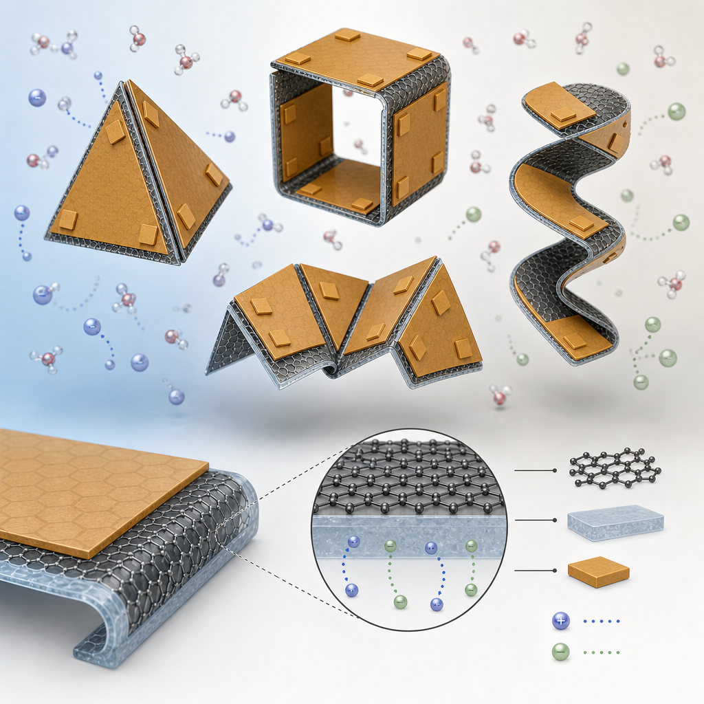
Researchers at Cornell University used CVD graphene grown on copper foil from ACS Material to demonstrate the world's smallest origami machines, combining the graphene with a 2-nm-thick atomic-layer-deposited silicon dioxide film to form a bimorph actuator only nanometers thick. The resulting devices fold into programmed 3D structures—tetrahedra, helices, cubes, clasps, and Miura-fold vertices—at the 10–50 µm scale, lift photoresist panels equivalent in mass to a 500-nm-thick silicon chip, and reversibly fold in under 100 ms when crossing a tunable pH threshold. The work, published in PNAS in 2018, opens a path to cell-sized autonomous machines for sensing, robotics, and biological interaction.
Self-folding sheets have become a powerful route to 3D microfabrication, but existing platforms based on polymers or shape-memory alloys are limited in how thin they can be made before losing stiffness, conductivity, or actuation strength. Reaching the cellular size regime—on the order of a red blood cell—requires structural layers that are both mechanically robust and electronically functional at nanometer thicknesses. Inorganic 2D materials like graphene are uniquely suited because they retain extreme stiffness, conductivity, chemical resistance, and thermal stability when scaled to atomic thickness. Demonstrating that such atomically thin sheets can drive useful folding behavior, carry payloads compatible with semiconductor processing, and respond reversibly to environmental stimuli is a key step toward microscale robotics with embedded photonic, electronic, or chemical functionality.
The Cornell team built their bimorphs by depositing a sacrificial aluminum or Al2O3 release layer onto fused silica coverslips, growing a 2-nm-thick SiO2 layer by plasma-enhanced atomic layer deposition at 200 °C, and then wet-transferring CVD-grown polycrystalline graphene from copper foil obtained from ACS Material. The Methods section states that "all of the devices are fabricated using polycrystalline graphene grown by chemical vapor deposition (ACS Material), with typical grain sizes ranging from 1 to 5 µm." PMMA-supported transfer was followed by ferric chloride etching of the copper, deionized water rinsing, lamination onto the SiO2/release stack, and PMMA removal by acetone soak. Patterning used photolithography, with O2 plasma to etch graphene and CF4 plasma to etch the SiO2. Rigid 2-µm-thick SU8 panels were then patterned on top to localize bending to defined hinge regions, and the bimorphs were released by HCl etching of the aluminum.
The bimorphs bend elastically to radii of curvature in the 1–5 µm range under strains of only ~10⁻⁴, two orders of magnitude below the SiO2 fracture threshold. Cross-sectional STEM/EELS confirmed the targeted 2-nm SiO2 thickness, and dark-field TEM characterized the graphene grain structure. The graphene–glass stack has a measured thermal expansion mismatch of 2 × 10⁻⁶/K, producing controllable curling between 40 °C and 160 °C. Bimorphs also respond chemically via Na⁺/H₃O⁺ ion exchange in the glass, unfolding sharply above pH 9 (or above pH 3 ± 1 in 1 M NaCl), with the transition fit by an equilibrium constant pK = 3.5. Folding and unfolding occur in under 0.5 s and 4 s respectively, an actuation speedup of roughly 10⁶ versus micrometer-thick films because diffusion times scale with thickness squared. The graphene retains a sheet resistance of about 1 kΩ/square in the bent state with typical electrolyte-gated response, and the bimorphs generate enough torque to lift SU8 panels 1,000 times thicker than themselves—mass-equivalent to a 500-nm silicon chip. Demonstrated structures include 20-µm tetrahedra, 50-µm cubes, programmable-pitch helices, interdigitated clasps, and Miura-fold vertices.
These results establish atomically thin hard-material origami as a platform for micrometer-scale robotics. Because the tetrahedron fits within a 12-µm sphere and responds in ~100 ms—comparable in size and timescale to cardiac cells and microorganisms—the devices are positioned for applications in cellular biophysics, targeted sensing, drug delivery vehicles, and reconfigurable photonic structures. The authors note that with 50-nm lithography, a full Intel 4004 microprocessor could fit on one face of a tetrahedron, and a 128-bit RFID chip could fit on a cube panel, suggesting integration with flexible electronics, embedded memory, and on-board communication. Follow-up work targets higher device yield, sequential and bidirectional folding schemes, and biocompatible deployments enabled by the low intrinsic toxicity of graphene, SiO2, and SU8.
For researchers building 2D-material actuators, microelectromechanical systems, or biointerfacing microrobots, the quality of the starting graphene is critical: uniform monolayer coverage, micrometer grain size, and clean transfer are all preconditions for elastic bending without fracture and for reproducible electrical performance after folding. ACS Material's CVD Graphene on Copper Foil, the source used in this study, is available to researchers pursuing similar bimorph, origami, and flexible electronics work.How ACS Material products were used
- CVD Graphene on Copper Foil (CVD Graphene) — “All of the devices are fabricated using polycrystalline graphene grown by chemical vapor deposition (ACS Material), with typical grain sizes ranging from 1 to 5 µm.”
Product Performance in this Study
The CVD graphene served as the conductive, atomically thin layer of the bimorph actuator. It bent elastically to micrometer radii while preserving its electrical conductivity (~1 kΩ/sq) and provided sufficient stiffness, paired with a 2-nm SiO2 layer, to lift rigid SU8 panels and enable folding into 3D origami structures.
Related product categories
Frequently asked questions
Why is CVD graphene used in microscale bimorph actuators?
CVD graphene combines an elastic modulus near 1,000 GPa with atomic thickness, allowing it to bend to micrometer radii without fracture while keeping its electrical conductivity. In the Cornell PNAS study, polycrystalline CVD graphene paired with a 2-nm SiO2 layer produced bimorphs that bend at strains of only 10⁻⁴, two orders of magnitude below the fracture threshold, and retained a sheet resistance of about 1 kΩ/square in the bent state.
How does pH trigger folding in graphene–glass bimorph origami?
The thin SiO2 layer exchanges Na⁺ and H₃O⁺ at dangling Si–O bonds. Large hydronium ions swell the glass and strain the bimorph, curling it. When the pH rises above a critical value (~9 in pure water, ~3 in 1 M NaCl), sodium replaces hydronium, the swelling vanishes, and the device flattens. The transition is reversible, follows an equilibrium with pK ≈ 3.5, and completes in under 0.5 seconds.
What payloads can graphene bimorph origami structures carry?
Although the graphene–glass bimorph is only nanometers thick, it can lift SU8 panels 2 µm thick—1,000 times its own thickness and mass-equivalent to a 500-nm silicon chip. This is enough to support photonic structures, chemical and biological samples, or microelectronic components. The authors estimate that an Intel 4004 microprocessor or a 128-bit RFID chip could be integrated onto a single folded panel.