-
CVD Graphene Electrode Ageing & Reliability — Soochow University, 2014
Jun 08, 2026 | ACS MATERIAL LLCShi, Y. et al. (2014). Ageing mechanisms and reliability of graphene-based electrodes. *Nano Research*.
Nano Research · 2014
Soochow University researchers used CVD graphene on copper from ACS Material to study ageing mechanisms and oxidation-induced Ohmic-to-Schottky transitions in graphene electrodes.
About this research
Researchers at Soochow University used CVD graphene single-layer (GSL) on copper foil purchased from ACS Material to develop the first in-depth ageing and reliability methodology for graphene-based electrodes, revealing that an ultra-thin oxide layer forms on pristine graphene and shifts the electrode's conduction mode from Ohmic to Schottky. The study, published in Nano Research in 2014 by Y. Shi, Y. Ji, F. Hui, H.-H. Wu, and M. Lanza of the Institute of Functional Nano & Soft Materials, combines accelerated oxidative testing, nanoscale conductive atomic force microscopy (CAFM), device-level graphene field-effect transistor (GFET) measurements, Weibull probabilistic analyses, and Fowler–Nordheim/Direct-Tunneling simulations to quantify how oxidation degrades graphene electrode performance.
Flexible transparent electrodes are widely recognized in the graphene technology roadmap as the central challenge for carbon electronics over the coming years. Applications range from displays, e-paper, and touchscreens to solar cells and wearable electronics, where graphene's combination of conductivity, transparency, and mechanical flexibility outperforms ITO and other candidates. However, while many studies have characterized graphene's intrinsic properties or run incipient anti-oxidation tests, no rigorous reliability framework existed for evaluating how graphene electrodes age under realistic operational conditions. Without such methodology, transitioning graphene from lab prototypes to industrial devices remains risky. This paper addresses that gap by introducing a disruptive, transferable workflow applicable to graphene as well as other carbon-based and two-dimensional materials.
The ACS Material CVD graphene single layer on copper served as the central test platform. According to the manufacturer, the GSL sheets are grown directly on copper foil by chemical vapor deposition, producing graphene domains 3–10 μm in diameter — a specification the authors directly observed and exploited in their SEM and AFM analyses. The pristine GSL/Cu stacks were subjected to accelerated oxidative ageing by immersion in 30% hydrogen peroxide for 1, 4, and 10 hours, a treatment previously shown to be equivalent to more than three months of atmospheric exposure. To fabricate GFETs, graphene was transferred from the ACS Material copper foil to n-type Si/SiO2 (300 nm) substrates using a standard PMMA-assisted wet transfer: PMMA spin coating at 2000 rpm, backside graphene removal via plasma, FeCl3 copper etching, HCl and water cleaning, substrate placement, and acetone removal. Gold electrodes (100 μm × 100 μm, 50 nm thick) were patterned by photolithography, e-beam evaporation, and lift-off.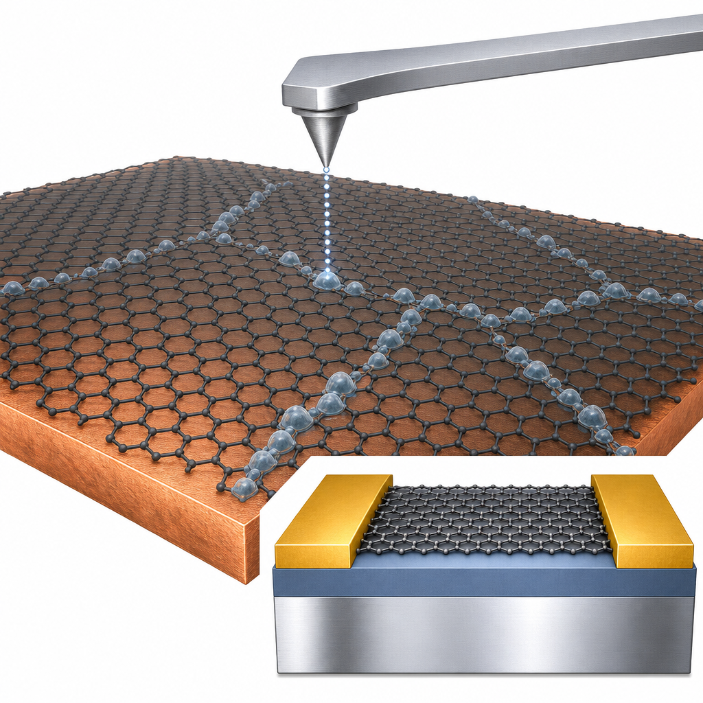
Multimodal characterization showed that H2O2 treatment produced dense surface hillocks that increased with soaking time, preferentially nucleating at graphene domain boundaries roughly 5 μm in diameter — matching the CVD domain size from the manufacturer specification. After 4 hours, hillock density stabilized, and at 10 hours oxidation propagated along graphene grain boundaries as widened oxidized paths. EDAX and XPS surveys confirmed elevated oxygen content at hillocks. UV–vis spectroscopy showed that transparency of the GSL film decreased substantially with treatment time, a critical metric for transparent electrode applications. CAFM I–V measurements collected with Pt–Ir-coated SCM-PIC tips at 20 nN contact force revealed that pristine plateau regions display Ohmic behavior, while oxidized regions developed clear Schottky-like rectifying characteristics. Tunneling current simulations based on Fowler–Nordheim and Direct-Tunneling models matched the experimental I–V data and corroborated the formation of an ultra-thin oxide barrier on the graphene surface. Weibull statistical analyses across the device population quantified the yield distribution, providing a probabilistic reliability metric usable in industrial qualification. GFET transfer curves confirmed degradation in carrier mobility and on/off behavior consistent with the nanoscale findings.
This methodology has direct implications for the commercialization of graphene-based transparent and flexible electrodes in displays, touchscreens, photovoltaics, and wearable sensors. By demonstrating that an unavoidable native oxide alters interface physics, the work pushes device designers to incorporate Schottky-barrier effects into circuit models or to develop encapsulation strategies that suppress surface oxidation. The framework is also extensible to other 2D materials including h-BN, MoS2, and WSe2, where similar ambient-induced degradation phenomena are increasingly reported. The authors propose that any roadmap toward mass production of carbon-based devices must include this type of accelerated ageing, multiscale characterization, and probabilistic modeling.
For researchers tackling similar reliability questions, CVD graphene on copper foil from ACS Material — the exact material used in this study — is available through the company's CVD Graphene catalog, alongside graphene transferred to SiO2, quartz, PET, and other substrates. The consistency of CVD domain size and transferability demonstrated here makes this product a practical starting point for groups studying transparent electrodes, GFETs, or 2D-material ageing under realistic environmental stress.How ACS Material products were used
- CVD Graphene on Copper Foil (Graphene Single Layer / GSL on Cu) (CVD Graphene) — “We used graphene single layer (GSL) on copper purchased from ACS Material. According to the manufacturer, GSL sheets are grown directly on copper by CVD, leading to graphene domain sizes with diameters around 3–10 μm.”
Product Performance in this StudyThe ACS Material CVD graphene-on-copper served as the primary test sample throughout the entire study. Its CVD-grown domain structure (3–10 μm) was directly observable in SEM/AFM imaging and was central to identifying how oxidation propagates along graphene grain boundaries. The product behaved consistently with manufacturer specifications, enabling reliable accelerated ageing analysis.
Related product categories
Frequently asked questionsHow does oxidation change the electrical behavior of graphene electrodes?
Accelerated oxidation produces an ultra-thin oxide layer on the graphene surface, particularly at domain boundaries. This layer transforms the contact interface from Ohmic to Schottky behavior, meaning the electrode develops rectifying characteristics that were not present in pristine graphene. The change can be quantified using conductive AFM I–V curves and modeled accurately with Fowler–Nordheim and Direct-Tunneling equations.
Why is CVD graphene on copper preferred for transparent electrode research?
CVD graphene on copper offers the best quality-to-price ratio for mass production and can be transferred onto arbitrary substrates including transparent polymers, glass, and silicon wafers. The CVD process yields uniform single-layer films with characterizable domain sizes — typically 3–10 μm — making it suitable for reproducible reliability testing, GFET fabrication, and large-area flexible electrode applications.
What is accelerated oxidative testing and why is it used on graphene?
Accelerated oxidative testing immerses graphene samples in hydrogen peroxide (typically 30%) for hours to simulate months of atmospheric exposure. A 4-hour H2O2 bath produces oxidation equivalent to over three months in ambient air. This approach lets researchers rapidly evaluate device ageing, predict long-term reliability, and identify failure mechanisms before committing to lengthy real-world stability studies.