-
CVD Graphene Electrodes for 2D RRAM Encryption - KAUST, 2024
Jun 03, 2026 | ACS MATERIAL LLCHan, T. et al. (2024). Fully 2D Materials‐Based Resistive Switching Circuits for Advanced Data Encryption. *Advanced Functional Materials*. https://doi.org/10.1002/adfm.202403029
Institute of Functional Nano & Soft Materials (FUNSOM) Collaborative Innovation Center of Suzhou Nano Science & Technology Soochow University 199 Ren‐Ai Road Suzhou 215123 China · Advanced Functional Materials · 2024
KAUST and Soochow University built flexible, transparent G/h-BN/G resistive switching circuits using CVD graphene electrodes from ACS Material for true random number generation.
About this research
Researchers at King Abdullah University of Science and Technology (KAUST), in collaboration with Soochow University and the Changchun Institute of Optics, used CVD-grown multilayer graphene (3–5 layers) from ACS Material, LLC as the conductive electrodes in fully 2D-materials-based resistive switching circuits that function as a true random number generator (TRNG) for data encryption. The work demonstrates flexible, transparent, metal-free G/h-BN/G memristive crossbar arrays in which graphene forms the top and bottom electrodes and hexagonal boron nitride acts as the switching medium. The devices exhibit volatile threshold-type resistive switching with high cycle-to-cycle variability that nonetheless replicates consistently across devices, making them ideal entropy sources. The bitstrings generated passed all randomness tests from the National Institute of Standards and Technology (NIST).
Data encryption is a foundational requirement in modern electronics, and true random number generators are the building blocks that produce unclonable identifiers and one-time keys. Conventional CMOS-based TRNGs draw roughly 1 mW per bit, restricting their use to wired computers and data centers. With the proliferation of the internet-of-things, mobile and wearable objects increasingly produce data that must be encrypted on the fly using micro-batteries or energy harvesters. Resistive-switching-based TRNGs can operate below 1 µW per bit, but prior implementations relied on rigid phase-change, resistive, or magnetic memory platforms. Realizing such circuits with flexible and transparent 2D materials would extend encryption hardware to clothing, wearables, and glasses, addressing an open challenge in low-power, embeddable security electronics.
The ACS Material CVD graphene was supplied as a 3–5 layer film grown on 25 µm polycrystalline copper foil. The authors transferred the graphene by a wet PMMA-assisted method: PMMA was spin-coated onto the graphene/Cu, baked at 100 °C, and the copper etched in saturated FeCl3 solution, followed by HCl and deionized water cleaning to remove residual Fe3+. The PMMA/graphene stack was lifted onto a 280 nm SiO2/Si wafer or a PET substrate and the PMMA dissolved in acetone. The bottom graphene was patterned by photolithography and oxygen plasma etching (300 W, 7 min) to form the bottom electrodes; multilayer h-BN was then transferred as the dielectric, and a second graphene sheet was transferred and patterned as the top electrodes. The resulting 10 × 10 crossbar arrays contained individual G/h-BN/G devices of 3 µm × 3 µm. For RS applications, the authors note the graphene electrodes need only be highly conductive, and the CVD-grown, defect-rich material suited the device requirements without demanding ultra-high crystalline quality.
The G/h-BN/G devices showed forming-free, threshold-type resistive switching with a sharp current rise above approximately 6 V and a 100 nA current compliance. Statistical analysis across 40 devices and 1025 cycles gave a set voltage of 6.04 ± 0.79 V and a reset voltage of 1.35 ± 0.44 V, with cycle-to-cycle variability comparable to device-to-device variability, exactly the balance required for entropy sources. Below 1 V the pristine current was under 1 pA, indicating a highly resistive off-state, and the low-resistance state fell between 1 and 10 MΩ. The graphene wire resistance measured just 16 Ω and could drive currents up to 300 µA. Cross-sectional TEM and EELS confirmed continuous graphene electrodes sandwiching the boron and nitride signals, with metal-free filamentary switching. On flexible PET substrates, devices retained their electrical behavior after bending 50 and 100 times at a 0.7 cm radius. Optical transmittance of the multilayer G and h-BN stacks exceeded 95%, and roughly 85% including the PET substrate. The high stochasticity of the G/h-BN/G devices allowed the generated bitstrings to pass all NIST randomness tests, in contrast to lower-variability Ag/h-BN/Ag devices.
This work enables low-power, flexible, and transparent hardware security primitives that could be embedded in internet-of-things devices, wearables, smart clothing, and optoelectronic systems. Because all 2D layers are produced by industry-compatible chemical vapor deposition, the platform can in principle be scaled to wafer dimensions, easing industrial adoption. The transparent conductive G/h-BN stacks are also suited to displays and energy applications. The authors frame the study as a proof-of-concept and note that application-specific transparency and endurance targets for flexible devices remain to be standardized, pointing toward integration with 2D or organic field-effect transistor peripheral circuitry for complete encryption systems.
For researchers pursuing 2D electronics, memristors, or flexible security hardware, this study shows that commercially available CVD multilayer graphene on copper foil can serve directly as device electrodes after standard wet transfer. The CVD graphene on copper foil used here is part of ACS Material's CVD graphene catalog, available to laboratories working on resistive switching, transparent conductors, and related 2D-material devices. The paper's results indicate that defect-rich CVD graphene is suitable for electrode roles where high conductivity, not pristine crystallinity, is the governing requirement.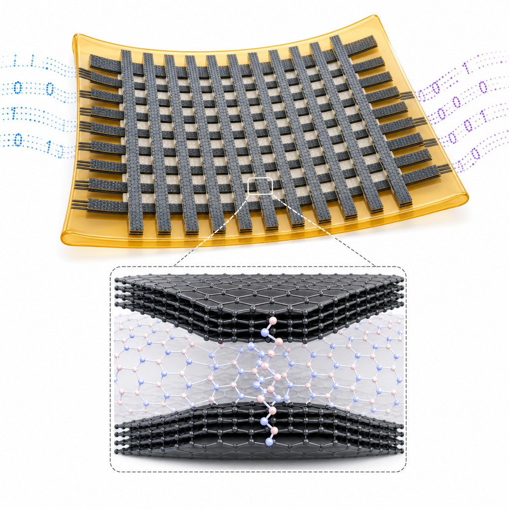
How ACS Material products were used
- CVD Graphene on Copper Foil (multilayer, 3–5 layers) (CVD Graphene) — “a graphene sheet with a thickness of 3–5 layers (from ACS Material, LLC) have been grown by CVD method on polycrystalline Cu foils”
Product Performance in this Study
The ACS Material CVD multilayer graphene served as both the top and bottom conductive electrodes in the G/h-BN/G threshold-type resistive switching devices. The graphene wires were highly conductive (16 Ω) and drove currents up to 300 µA, sufficient to operate the metal-free TRNG circuit on both rigid and flexible substrates.
Related product categories
Frequently asked questions
What role does CVD graphene play in G/h-BN/G resistive switching devices?
In this study, CVD-grown multilayer graphene (3–5 layers) served as both the top and bottom electrodes of the G/h-BN/G resistive switching devices. The graphene wires were highly conductive, with a measured resistance of 16 Ω, and could drive currents up to 300 µA. Hexagonal boron nitride acted as the switching medium between the two graphene electrodes in a metal-free vertical structure.
Why is CVD graphene preferred over exfoliated graphene for these flexible devices?
CVD graphene can be grown at wafer scale with relatively low thickness fluctuations, making it the preferred synthesis route for industry. For resistive switching electrodes the material only needs to be highly conductive, not pristine, so the defect-rich nature of CVD graphene is acceptable. Its scalability and compatibility with standard transfer and lithography processes enabled fabrication of 10 × 10 crossbar arrays on both SiO2/Si and flexible PET.
How does the variability of G/h-BN/G devices enable random number generation?
The G/h-BN/G devices show high cycle-to-cycle variability in switching voltage and resistance, yet this variability is consistent across devices. Across 40 devices and 1025 cycles the set voltage was 6.04 ± 0.79 V. This balance of stochasticity and reproducibility makes the devices reliable entropy sources, and the resulting bitstrings passed all NIST randomness tests, unlike lower-variability Ag/h-BN/Ag devices.