-
CVD Graphene for Blue Luminescence Study - NYCU, 2024
Jun 29, 2026 | ACS MATERIAL LLCLin, S. et al. (2024). Blue Luminescence from N-doped Graphene. *The Astrophysical Journal*. https://doi.org/10.3847/1538-4357/ad98e8
The Astrophysical Journal · 2024
Researchers at National Yang Ming Chiao Tung University used ACS Material single-layer CVD graphene to model interstellar blue luminescence via N-doping.
About this research
Researchers at National Yang Ming Chiao Tung University, working with the National Synchrotron Radiation Research Center, used single-layer CVD graphene purchased from ACS Material to reproduce the astrophysical blue luminescence (BL) observed in the Red Rectangle Nebula. By exposing the pristine graphene films, coated with solid N2 at cryogenic temperature, to vacuum ultraviolet (VUV) radiation, the team generated nitrogen-doped graphene whose photoluminescence (PL) peaks at 378 nm—nearly identical to the 375 nm BL band seen in space. This provides a laboratory analog for a long-debated interstellar emission, offering an alternative to the small polycyclic aromatic hydrocarbon (PAH) hypothesis.
Blue luminescence is a near-UV/visible emission feature spatially correlated with aromatic infrared emission in several reflection nebulae. For two decades, small PAHs such as anthracene and pyrene have been the leading candidate carriers, but a complete and self-consistent identification has remained elusive. The extended red emission (ERE) and BL were both first discovered in the Red Rectangle, hinting at a related carbonaceous chemical origin. Building on prior work proposing VUV-processed graphene and graphene quantum dots as ERE carriers, this study tests whether heteroatom-doped graphene can match BL. The question matters for astrochemistry and laboratory astrophysics because identifying the carriers of unidentified interstellar emissions constrains the inventory and processing of carbonaceous dust in the interstellar medium.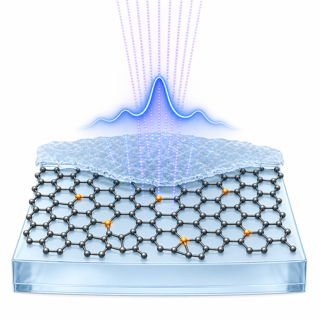
The ACS Material product is central to the methodology. The authors state that "pristine SLG thin films were purchased from ACS Material; these thin-film samples were prepared using chemical vapor deposition followed by wet transfer onto MgF2 substrates (2 mm thick, Crystran)." Each graphene sample measured 1 × 1 cm2 on a 1 inch optical substrate. The MgF2-mounted graphene was attached to the cold finger of a cryostat (RDK-415D) and cooled to 10 K, where roughly 20 layers of solid N2 or O2 were deposited (about 0.5 sccm for 5 s). The film was then irradiated for 2 hr at 121.6 nm using the TLS-21A2 beamline at the Taiwan Light Source, with a photon flux of about 10^15 photons s^-1 in a 2 mm spot. Raman spectroscopy of the pristine film confirmed monolayer graphene quality, showing G and 2D bands at 1584 and 2682 cm^-1 and only a weak D band, demonstrating that the ACS Material graphene provided a clean, low-defect baseline for the doping experiments.
The key results are quantitative and spectrally precise. Upon 121.6 nm excitation, the N2-covered (N-doped) graphene produced an asymmetrical PL band peaking at 378 nm with a full width at half maximum of 50 nm and a shoulder near 396 nm—matching both the band position (observed BL peak at 375 nm) and asymmetric shape of the nebular emission. In contrast, the O2-covered (O-doped) sample showed a symmetrical PL band at 416 nm with a narrower 30 nm bandwidth, which does not match BL. Commercially obtained N-doped graphene and graphene oxide flakes (Sigma-Aldrich, Hummers' method) were measured for comparison and showed bands redshifted by 30 nm and 45 nm respectively, with broader, less well-defined shoulders. Raman spectra of the doped films exhibited strong D, D', and D+D' bands, indicating structural and impurity defects; the strong D' band in the N2 sample signaled that nitrogen substitutes carbon in the lattice rather than functionalizing externally. XPS of the N-doped sample showed a single N 1s band deconvoluting into pyrrolic-N (400.1 eV) and pyridinic-N (398.0 eV) components, while the O-doped sample showed O 1s components at C–O–C (533.5 eV), C–OH (532.8 eV), and O–C=O (531.0 eV). The simplicity of the N-bonding structure supports N-doped graphene as a clean model carrier.
This research enables a new framework for interpreting interstellar emission features. Because the central region of the Red Rectangle has an oxygen-rich disk, the authors suggest the observed spectrum may arise from a mixture of N- and O-doped graphene, with N-doping the dominant contributor. The photochemical approach also offers a general route to introduce diverse heteroatoms and functional groups into graphene, extending beyond N and O, so that graphene can serve as a tunable laboratory analog for astrochemical spectroscopy. Planned follow-up work includes exposing graphene covered by mixed N2/O2 ices to VUV light and exploring gas-phase nitrogen-incorporation pathways. Beyond astrophysics, the same controllable defect-and-dope strategy is relevant to graphene photonics, luminescent carbon materials, and defect-engineered 2D devices.
For researchers pursuing similar studies, the work shows that high-quality single-layer CVD graphene is a reliable substrate for defect-engineering and heteroatom-doping experiments demanding clean, reproducible starting material. The single-layer CVD graphene used here is available from ACS Material's CVD graphene catalog, where graphene-on-various-substrate and transfer-ready formats support photoluminescence, Raman, and XPS-based investigations in laboratory astrophysics, 2D-materials photonics, and defect-engineering research.How ACS Material products were used
- Single-layer CVD graphene thin film (wet-transferred onto MgF2 substrate) (CVD Graphene) — “Pristine SLG thin films were purchased from ACS Material; these thin-film samples were prepared using chemical vapor deposition followed by wet transfer onto MgF2 substrates (2 mm thick, Crystran). The dimensions of the graphene samples were 1 × 1 cm2 on a 1 inch diameter optical substrate.”
Product Performance in this StudyThe ACS Material single-layer CVD graphene served as the pristine starting material that was photochemically converted into N- and O-doped graphene. Raman confirmed high-quality monolayer graphene (sharp G and 2D bands, weak D band), making it a clean platform for studying doping-induced luminescence.
Related product categories
Frequently asked questionsWhy is single-layer CVD graphene used to model interstellar blue luminescence?
Single-layer CVD graphene offers a clean, low-defect carbon network that can be controllably modified by VUV irradiation. In this study, pristine graphene from ACS Material was coated with solid N2 and irradiated at 121.6 nm to create N-doped graphene, whose 378 nm photoluminescence closely matches the 375 nm blue luminescence observed in the Red Rectangle Nebula, making it a faithful laboratory analog.
How does nitrogen doping change the photoluminescence of graphene?
Nitrogen substitution introduces structural defects and pyrrolic-N and pyridinic-N bonding into the graphene lattice, confirmed by Raman and XPS. This produces an asymmetrical photoluminescence band peaking at 378 nm with a 50 nm full width at half maximum and a shoulder near 396 nm, distinctly different from O-doped graphene, which shows a symmetric 416 nm band.
What grade of graphene is best for defect-engineering and luminescence experiments?
High-quality monolayer CVD graphene, wet-transferred onto a transparent substrate such as MgF2, is ideal because Raman confirms strong G and 2D bands with only a weak D band before processing. This clean baseline ensures that any defects and luminescence observed after doping arise from the experiment rather than the starting material.