-
CVD Graphene for Flexible Microsupercapacitors - University of Akron, 2021
Jun 26, 2026 | ACS MATERIAL LLCYang, M. et al. (2021). Molecular ENGINEERING of polyaniline with ultrathin polydopamine and monolayer graphene for all-solid-state flexible microsupercapacitors. *ACS Applied Energy Materials*. https://doi.org/10.1021/acsaem.1c01996
The University of Akron · ACS Applied Energy Materials · 2021
University of Akron researchers used ACS Material CVD graphene as a substrate for PANI/PDA microsupercapacitors, raising areal capacitance to 4.6 mF/cm2.
About this research
Researchers at The University of Akron used CVD graphene purchased from ACS Material, LLC as an atomically thin conductive substrate for the in situ polymerization of polyaniline (PANI), producing all-solid-state flexible microsupercapacitors (MSCs) whose graphene-templated electrodes reached an areal capacitance of 4.6 mF/cm2 and a gravimetric capacitance of 107.0 F/g at 5 mA/cm2. The work introduces a reactive layer-by-layer (LbL) deposition strategy in which alternating PANI and ultrathin polydopamine (PDA) layers, plus a continuous monolayer graphene template, are combined with lithography patterning to make interdigitated micro-devices. The combined approach tunes PANI structure at the molecular level and improves capacitance, mechanical flexibility, and cycling stability.
Miniaturized, flexible energy storage is increasingly important for soft electronics, wearable sensors, and robotics. In-plane MSCs with interdigitated electrodes offer high power density, fast charge/discharge, and easy on-chip integration. Conducting polymers such as PANI are attractive pseudocapacitive materials because of high specific capacitance, flexibility, and low cost, but they suffer from poor cycling stability and limited potential windows caused by swelling and structural degradation. Mixing PANI with carbon nanomaterials or metal oxides helps but does not address molecular-level structure control. This paper targets that open challenge by using a biobased adhesive (PDA) and a graphene template to reshape PANI molecular packing and morphology without bulk inorganic additives, an approach relevant to long-tail searches around flexible supercapacitor electrodes and conducting-polymer energy storage.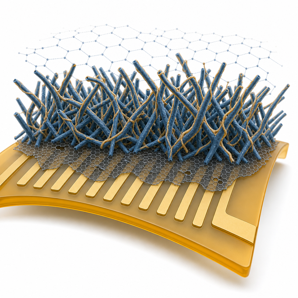
The ACS Material CVD graphene was transferred and patterned onto the device substrate before PANI deposition, as described in the Experimental Section: "The fabrication of G-PANI MSC follows the same procedure, except that there was an additional CVD graphene transfer and patterning step before the deposition of PANI layer." Aniline was then polymerized directly on top of the graphene at low temperature (−20 C, 3.5 h) in formic acid and NaCl with ammonium persulfate as oxidant. Raman characterization of the graphene showed sharp G and 2D bands with a high I2D/IG ratio, confirming high-quality monolayer material; AFM measured a thickness near 1.0 nm. Because the hydrophobic monolayer graphene, with intrinsic defects and wrinkles, acts as a template, the resulting G-PANI1 film had a higher root-mean-square roughness (82 nm) than PANI on bare substrate (34 nm) over a 7x7 um area, while keeping a similar nanofiber network morphology and overall thickness. The graphene served as the conductive base layer enabling a meaningful electric double-layer contribution alongside PANI pseudocapacitance.
Introducing the monolayer graphene substrate markedly improved electrochemical behavior. Cyclic voltammetry at 100 mV/s showed the G-PANI1 device with a more rectangular CV curve, shifted redox peaks, and a larger enclosed area than PANI1, indicating added double-layer capacitance. Galvanostatic charge/discharge at 1 mA/cm2 gave a near-triangular curve with almost no IR drop for G-PANI1, versus a distorted curve and large IR drop for PANI1, signaling lower internal resistance. At 5 mA/cm2, areal capacitance rose from 3.4 to 4.6 mF/cm2 and gravimetric capacitance from 77.5 to 107.0 F/g when graphene was used. EIS Nyquist plots showed G-PANI1 with essentially no high-frequency semicircle and a steeper low-frequency slope, indicating reduced charge-transfer resistance. Separately, the PDA-engineered electrodes performed strongly: areal capacitances of PANI2, (PANI-PDA)1.5, and (PANI-PDA)2 at 5 mA/cm2 were 25.9, 31.0, and 33.2 mF/cm2, with gravimetric values of 65.0, 86.4, and 84.1 F/g. The (PANI-PDA)1.5 device retained 74% capacitance after 1000 cycles (71% after 2000), improving on the PANI2 control (65%), and kept 95% capacitance retention at a 120 degree bending angle. GIWAXS confirmed smaller PANI d-spacings after PDA insertion, linking molecular packing to performance.
The results enable flexible, miniaturized energy storage components for on-chip electronics, wearable devices, sensors, and soft robotics, where small footprint and bending tolerance are essential. The reactive LbL approach is substrate-agnostic, working on rigid silicon wafers and flexible polyimide, and the interdigital geometry (finger width, spacing, count) can be tuned by photomask design. The authors demonstrate series and parallel device interconnection to scale operating voltage and current, pointing toward integrated MSC arrays. They also note that combining the (PANI-PDA)n electrodes with inorganic nanomaterials could further raise cycling stability, defining a clear path for hybrid electrode development in conducting-polymer supercapacitors.
For researchers pursuing similar flexible-electrode and conducting-polymer work, the continuous, high-quality monolayer CVD graphene used here as a polymerization template is the type of material available from ACS Material's CVD graphene line. The paper shows that a well-transferred monolayer graphene base can lower charge-transfer resistance and boost both areal and gravimetric capacitance without bulk additives, making it a practical option for groups building thin-film, on-chip, or wearable energy storage devices. As always, performance depends on transfer quality and device design, but the data here support graphene's role as an effective conductive substrate.How ACS Material products were used
- CVD Graphene (monolayer, transferred onto device substrate) (CVD Graphene) — “CVD graphene was purchased from ACS Material, LLC.”
Product Performance in this StudyUsed as an atomically thin conductive substrate for in situ aniline polymerization; the monolayer graphene reduced charge-transfer resistance and improved areal/gravimetric capacitance and cycling stability of the PANI-based microsupercapacitor.
Related product categories
Frequently asked questionsHow does monolayer CVD graphene improve polyaniline microsupercapacitor performance?
Used as an atomically thin conductive substrate for in situ aniline polymerization, the monolayer graphene adds an electric double-layer contribution to PANI pseudocapacitance and reduces charge-transfer resistance. In this study it raised areal capacitance from 3.4 to 4.6 mF/cm2 and gravimetric capacitance from 77.5 to 107.0 F/g at 5 mA/cm2, while eliminating most of the IR drop in charge/discharge curves and improving stability.
What is CVD graphene used for in flexible energy storage devices?
In flexible all-solid-state microsupercapacitors, CVD graphene serves as a continuous, large-area, conductive template onto which active materials like polyaniline are grown. Its low sheet resistance and intimate contact with the polymer film improve charge transfer efficiency and reduce current leakage, enabling thinner electrodes with better cycling stability and bending tolerance for on-chip and wearable applications.
Why is low charge-transfer resistance important for microsupercapacitor electrodes?
Lower charge-transfer resistance allows faster ion and electron movement at the electrode interface, producing near-triangular galvanostatic charge/discharge curves with minimal IR drop and higher usable capacitance at high current densities. In this work, the graphene-templated electrode showed almost no high-frequency semicircle in EIS, confirming reduced resistance and improved rate performance compared with PANI on a bare substrate.