-
CVD Graphene for Infrared Near-Field Microscopy - RWTH Aachen, 2014
Jun 12, 2026 | ACS MATERIAL LLCLi, P. et al. (2014). Graphene-enhanced infrared near-field microscopy. *Nano Letters*. https://doi.org/10.1021/nl501376a
RWTH Aachen University · Nano Letters · 2014
RWTH Aachen researchers used CVD monolayer graphene from ACS Material to boost infrared near-field microscopy, resolving buried structures at λ/11 resolution.
About this research
Researchers at RWTH Aachen University demonstrated, using CVD monolayer graphene supplied by ACS Material, that a single atomic layer of graphene can deliver a 7-fold enhancement of evanescent fields in infrared near-field microscopy, enabling λ/11-resolution imaging of structures buried 500 nm below the sample surface. The work, published in Nano Letters in 2014 by Li, Wang, Böckmann, and Taubner, provides the first experimental verification of long-predicted graphene-enhanced subsurface imaging. By transferring a heavily doped monolayer onto buried gold features and probing the system with a scattering-type SNOM at 9.2–11.3 μm, the team confirmed that graphene plasmonics can rescue otherwise inaccessible subwavelength information.
Optical microscopy is fundamentally diffraction-limited because evanescent fields carrying subwavelength information decay within a fraction of a wavelength from the source. Scattering-type near-field optical microscopy (s-SNOM) recovers these fields with a sharp tip but loses contrast rapidly when the feature of interest is buried tens to hundreds of nanometers below the surface. Conventional superlenses solve this in principle but require resonant negative-permittivity slabs that are difficult to fabricate over arbitrary samples. A practical, transferable, broadband alternative would benefit applications ranging from semiconductor nanowire doping profiling and growth-defect inspection to noninvasive imaging of subcellular structures. Graphene, with its strongly confined and tunable plasmons, is an attractive candidate because it can be transferred onto essentially any sample without disturbing the underlying architecture.
The key material in the work was commercial monolayer graphene from ACS Material, grown by chemical vapor deposition on 25 µm copper foils. The authors state in the Methods that "Commercial monolayer graphene (ACS MATERIAL, LLC) is prepared by CVD grown on 25 mm thick copper foils." A 500-nm PMMA film served two roles: as a transfer carrier and as a chemical n-dopant that pushed the graphene Fermi level high enough to support mid-infrared plasmons. Two geometries were tested: a graphene–PMMA configuration with graphene on top of the PMMA spacer, and a PMMA–graphene configuration with graphene directly adjacent to the buried gold structures. In both cases the CVD graphene supplied the plasmonic medium responsible for funneling high-k evanescent information toward the SNOM tip, with heavy doping intentionally suppressing propagating plasmons and emphasizing the non-resonant enhancement regime that proved less sensitive to graphene loss.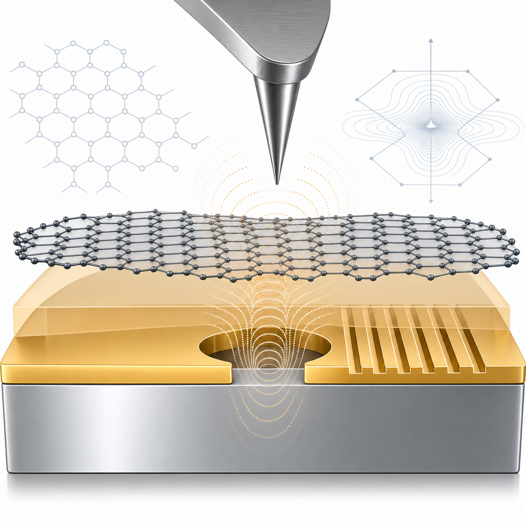
The central experiment imaged a 1.5-µm-diameter hole patterned in a 40-nm Au layer on Si and covered by the graphene/PMMA stack. Without graphene, the buried hole was essentially invisible at λ = 11.3 µm; with graphene, it was clearly resolved with an optical width of 1.3 ± 0.1 µm and contrast Δs/smax ≈ 0.11 at 11.3 µm, about three times the contrast at 10.2 µm. A graphene-covered Au grating (3.3-µm period, 1.5-µm gap) provided quantitative enhancement metrics from Fourier analysis of line scans: 1.8-fold enhancement of the first-order harmonic (kx = 3.8 k0), 3-fold for the second order (kx = 7.5 k0), and 7-fold for the third order (kx = 11.3 k0). The third-order harmonic was retrievable only above 10.7 µm, defining a working bandwidth of roughly 0.6 µm for the highest-resolution channel and a usable bandwidth above 1.1 µm overall. Transfer-matrix modeling with a Drude graphene sheet conductivity (EF = 0.6 eV, μ ≈ 3000 cm² V⁻¹ s⁻¹, εPMMA = 2.3) reproduced the kx- and λ-dependent transmittance, and showed that in the non-resonant regime (kx < kp) the enhancement is largely insensitive to carrier mobility, remaining stable from 800 to 8000 cm² V⁻¹ s⁻¹. This robustness against intrinsic loss is what makes CVD-grade graphene practical for the technique.
The demonstrated capability extends s-SNOM into application spaces previously inaccessible. The authors point to nondestructive mapping of free-carrier and doping profiles in buried semiconductor nanowires, subsurface defect detection during materials growth, and noninvasive infrared imaging of subcellular biological structures. They further outline extensions to multilayer graphene stacks for nanoscale resolution, gate- or chemically tunable graphene lenses spanning a wider mid-IR window for vibrational fingerprinting, and adaptation of the same mechanism to other 2D materials such as hexagonal boron nitride for phonon-polariton imaging. Because the enhancement layer is simply transferred onto the sample, the method is compatible with virtually any planar substrate, including industrial wafers and biological supports.
For researchers working on graphene plasmonics, near-field optics, subsurface metrology, or 2D-material heterostructures, CVD monolayer graphene on copper foil of the type used here is available from ACS Material, including the CVD Graphene on Copper Foil product line. The paper provides a useful benchmark: even unoptimized, heavily doped CVD graphene delivers a measurable 7-fold evanescent enhancement and λ/11 buried-feature resolution at mid-infrared wavelengths, with performance limited more by film cleanliness and transfer quality than by intrinsic graphene loss. Groups designing graphene hyperlenses, near-field lenses, or tunable IR imaging platforms can use commercial CVD graphene as a starting point for similar transferable, broadband enhancement layers.How ACS Material products were used
- CVD Graphene on Copper Foil (CVD Graphene) — “Commercial monolayer graphene (ACS MATERIAL, LLC) is prepared by CVD grown on 25 mm thick copper foils.”
Product Performance in this StudyThe monolayer CVD graphene from ACS Material served as the evanescent-field-enhancing layer at the heart of the experiment. After PMMA-assisted transfer onto buried test structures, the graphene produced a measurable ~7-fold enhancement of high-spatial-frequency near-field information, enabling λ/11 resolution of features buried 500 nm deep.
Related product categories
Frequently asked questionsHow does monolayer graphene enhance infrared near-field microscopy?
Monolayer graphene supports highly confined infrared plasmons that boost the transmission of high-spatial-frequency evanescent fields from a buried object up to the SNOM tip. In this Nano Letters study, transferring CVD graphene onto a PMMA-covered sample produced a 7-fold enhancement of the third-order grating harmonic at λ = 11.3 µm, allowing buried structures hidden under 500 nm of PMMA to be resolved that were otherwise invisible to the bare s-SNOM.
Why is heavily doped CVD graphene preferred for subsurface near-field imaging?
Heavy doping pushes the graphene Fermi level high enough (around 0.6 eV) to support mid-infrared plasmons and shifts the operating point into a non-resonant regime where kx < kp. In this regime the evanescent-field enhancement is largely insensitive to carrier mobility, so CVD graphene with mobilities of 800–3000 cm² V⁻¹ s⁻¹ delivers stable performance. Propagating plasmons that would distort the image are also suppressed, leaving a clean, broadband enhancement window.
What resolution can graphene-enhanced s-SNOM achieve for buried features?
The Aachen team resolved a 1.5-µm-diameter hole buried under 500 nm of PMMA at λ = 11.3 µm, corresponding to about λ/11 resolution in the mid-infrared. Fourier analysis of a 3.3-µm-period grating confirmed enhancements of 1.8×, 3×, and 7× for the first, second, and third-order harmonics, respectively. Performance is best at longer wavelengths, with a useful bandwidth above 1.1 µm and a third-harmonic window of roughly 0.6 µm.