-
CVD Graphene for NIR Photodetectors - Bose Institute, 2023
Jun 10, 2026 | ACS MATERIAL LLCMasanta, S. et al. (2023). Monolayer graphene–MoSSe van der Waals heterostructure for highly responsive gate-tunable near-infrared-sensitive broadband fast photodetector. *ACS Applied Materials & Interfaces*. https://doi.org/10.1021/acsami.2c20707
Bose Institute · ACS Applied Materials & Interfaces · 2023
Bose Institute built a MoSSe/graphene heterostructure photodetector on ACS Material CVD graphene, reaching 60 A/W responsivity and ~38 ms response at 800 nm.
About this research
Researchers at Bose Institute, Kolkata, used monolayer CVD graphene purchased from ACS Material, LLC, as the charge-transport channel of a MoSSe/graphene van der Waals heterostructure photodetector that achieved a responsivity of 0.6 × 10^2 A/W and detectivity of 7.9 × 10^11 Jones at 800 nm in ambient air. By pairing high-mobility graphene with an alloy transition-metal-dichalcogenide light absorber, the team demonstrated broadband (visible to near-infrared) detection spanning 400–1100 nm. The device also showed appreciable self-bias operation and fast switching, making it attractive for low-power, ambient-condition optoelectronics. The work combines bandgap engineering of the MoSSe alloy with the carrier-transport strengths of CVD graphene.
Two-dimensional van der Waals heterostructures are central to nanoscale photonics because they can combine complementary materials properties in atomically thin stacks. Pristine graphene offers ultrafast, broadband photoresponse but lacks a bandgap, giving weak optical responsivity, while TMDCs absorb strongly yet suffer from low carrier mobility that slows device speed. Combining the two overcomes both limitations, but the detection window is still capped by the TMDC bandgap, which usually restricts response to the visible range. Extending sensitivity into the near-infrared is important for telecommunications, night vision, biomedical imaging, and energy harvesting. Alloying MoS2 and MoSe2 into MoSSe lets the absorption edge be tuned toward the NIR, and the alloy's shallow-level trap states enhance photocarrier generation. The open challenge addressed here is achieving high NIR sensitivity, fast response, and low power consumption simultaneously, in ambient air rather than high vacuum.
The ACS Material product entered the workflow as monolayer CVD graphene grown on a p-type SiO2/Si substrate (300 nm SiO2 dielectric, highly p-doped Si back gate). The Experimental Section states the monolayer CVD graphene was purchased from ACS Material, LLC. A graphene channel 100 µm long and 30 µm wide was patterned by standard photolithography and oxygen-plasma etching. Ohmic contacts were formed by photolithography and thermal evaporation of 7 nm Ti and 70 nm Au. MoSSe crystal (from a separate supplier) was liquid-exfoliated in ethanol by 48 h ultrasonication in an ice bath, then centrifuged at 5000 rpm; the supernatant containing few-layer MoSSe flakes was drop-cast onto the graphene channel between source and drain electrodes to form the van der Waals heterostructure. The completed phototransistor was dried at 60 °C for 2 h and mounted on a PCB chip. Raman spectra confirmed the characteristic graphene G and 2D modes at 1595 and 2696 cm^-1, and a red shift of the 2D mode in the hybrid indicated photogenerated charge transfer from MoSSe into the graphene channel, validating graphene's role as the transport layer.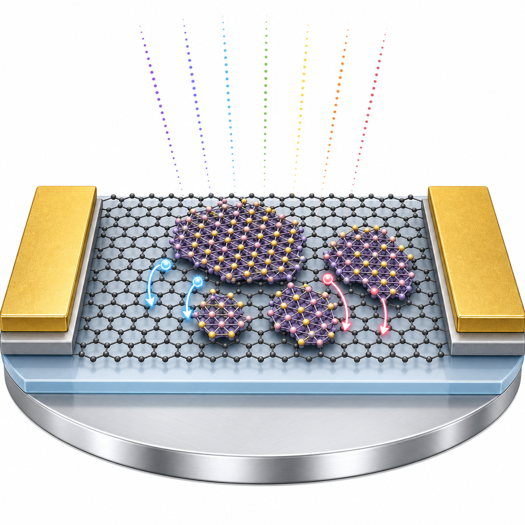
The device reached responsivity of 0.6 × 10^2 A/W and detectivity of 7.9 × 10^11 Jones at 800 nm under 17 fW/µm^2 power density and 10 mV source–drain bias. Carrier mobility of the hybrid was 0.78 × 10^2 cm^2 V^-1 s^-1. In self-bias mode (VDS = 0 V), the detector still produced a stable 10.78 A/W response at 800 nm and 830 fW/µm^2, arising from a built-in field due to nonuniform MoSSe distribution and electrode asymmetry. Applying a source–drain bias of 1 V raised responsivity to 3.24 × 10^2 A/W (about 30× the 1 mV value), with detectivity of 4.02 × 10^11 Jones and external quantum efficiency reaching 5.03 × 10^2. Gate tuning shifted responsivity up to 5-fold at VBG = 50 V and could switch the sign of the photocurrent across three doping regions. Temporal measurements gave fast rise/decay times of ~38 ms/~48 ms at VDS = 1 mV (~39 ms/~47 ms in self-bias mode), with reproducible switching over 1800 s and no persistent current. The noise-equivalent power reached as low as 6.9 × 10^-15 W·Hz^-1/2, photogain was 0.37 × 10^3, and the calculated maximum operating frequency, bandwidth, and gain–bandwidth product were 3.30 Hz, 7.30 Hz, and 2.7 kHz, respectively. A comparison table shows the device outperforms prior MoSSe and graphene/MoSSe detectors in ambient operability, spectral range, and speed.
This demonstration enables compact, low-power near-infrared and broadband photodetectors that function in ambient air without external bias, useful for energy-harvesting photodetectors, optical communication receivers, imaging arrays, and wearable or portable optoelectronic sensors. The combination of self-bias operation, gate-tunable responsivity sign, and fast switching points to multifunctional 2D photonic devices and logic-integrated detectors. The authors highlight the potential for next-generation energy harvesting and broadband photodetection, and the platform could be extended by varying MoSSe composition to fine-tune the spectral window or by integrating the graphene channel with other alloy TMDCs to further enhance NIR sensitivity and dynamic range.
For researchers pursuing similar 2D heterostructure devices, the monolayer CVD graphene on SiO2/Si used here is available from ACS Material as a ready-to-pattern transport channel. Its high carrier mobility and clean Raman signatures supported reliable phototransistor fabrication and gate-tunable charge transport in this study. Groups working on van der Waals photodetectors, flexible optoelectronics, and broadband sensing can source comparable CVD graphene substrates to reproduce or build on these results, with device performance ultimately governed by the heterostructure design and processing rather than by any single material alone.How ACS Material products were used
- Monolayer CVD Graphene on SiO2/Si Substrate (CVD Graphene) — “The MoSSe crystal and monolayer CVD graphene on a SiO2/Sip-type substrate were purchased from HQ Graphene (Groningen, The Netherlands) and ACS Material, LLC, respectively.”
Product Performance in this StudyThe ACS Material monolayer CVD graphene served as the high-mobility charge-transport channel of the photodetector, supporting a carrier mobility of 0.78 × 10^2 cm^2 V^-1 s^-1 and enabling fast, gate-tunable broadband photoresponse.
Related product categories
Frequently asked questionsWhy is CVD graphene used as the channel in a MoSSe photodetector?
CVD graphene provides a high-carrier-mobility transport channel that quickly collects photogenerated holes transferred from the MoSSe absorber. In this study the hybrid device reached a mobility of 0.78 × 10^2 cm^2 V^-1 s^-1, enabling high photoconductive gain and fast rise/decay times of about 38 ms and 48 ms, which pure TMDC channels cannot achieve due to slow carrier trapping.
What responsivity can a MoSSe/graphene heterostructure photodetector achieve in the near-infrared?
The reported device achieved a responsivity of 0.6 × 10^2 A/W and detectivity of 7.9 × 10^11 Jones at 800 nm under only 10 mV bias and 17 fW/µm^2 power density. Applying a 1 V source–drain bias raised responsivity to 3.24 × 10^2 A/W, while self-bias operation at zero bias still gave 10.78 A/W at 800 nm.
How does gate voltage tune the photoresponse of a graphene-based heterostructure detector?
The Si back gate controls the graphene channel's hole doping across three regions. In the lightly hole-doped region the device reaches its ON state with high positive photocurrent, and responsivity increased up to 5-fold at VBG = 50 V relative to zero gate bias. The gate can even switch the sign of the photocurrent, adding functional flexibility to the detector.