-
CVD Graphene for Quantum Dot Switching - LBNL, 2014
May 26, 2026 | ACS MATERIAL LLCLee, J. et al. (2014). Switching individual quantum dot emission through electrically controlling resonant energy transfer to graphene. *Nano Letters*. https://doi.org/10.1021/nl503587z
Nano Letters · 2014
Researchers at Lawrence Berkeley National Laboratory used ACS Material CVD graphene on copper to electrically switch individual PbS quantum dot emission at room temperature.
About this research
Researchers at Lawrence Berkeley National Laboratory's Molecular Foundry, working with collaborators at the University of California, Berkeley, used monolayer CVD graphene on copper foil purchased from ACS Material to demonstrate electrically controlled photoluminescence switching of individual colloidal quantum dots at room temperature. The team, led by Jiye Lee, Feng Wang, and Alexander Weber-Bargioni, showed that gating the graphene shifts its Fermi level by more than half the emitter excitation energy, suppressing interband transitions and turning off resonant energy transfer from PbS and PbS/CdS quantum dots. Peak photoluminescence intensity of 1.3 eV-emitting dots increased by ~50% at -5 V relative to 0 V, and the modulation followed the d^-4 distance scaling unique to energy transfer into a two-dimensional acceptor.
Why this research matters: Nano-emitters such as colloidal quantum dots are central building blocks for quantum optics, nanophotonic communication, and biological imaging, but switching their emission on demand at scales below the diffraction limit has been difficult. Previous voltage-controlled approaches relied on the quantum-confined Stark effect in epitaxial quantum dots, which is weak compared with the inhomogeneous broadening of colloidal emitters and typically requires cryogenic operation. Graphene offers an alternative: its optical transitions can be tuned across a broad spectrum by electrostatic doping, and Forster-like energy transfer into graphene is extremely efficient at sub-20 nm distances. A graphene-based nano-emitter switch could therefore work with solution-processable emitters of many bandgaps at ambient temperature, opening a path to integrated nanophotonic modulators and electrically addressable single-photon sources.
How the ACS Material product was used: The Methods section states explicitly that "monolayer graphene on copper foils was purchased from ACS Material or grown by chemical vapor deposition independently." The CVD graphene on copper foil served as the active two-dimensional acceptor layer in the device. PMMA was spin-coated on the as-received graphene/Cu, the copper was etched in 0.1 M ammonium persulfate, and the floating graphene/PMMA stack was transferred onto a single-crystal LaF3 (100) substrate that acts as a solid-state fluoride-ion electrolyte gate. After dissolving the PMMA in acetone, the graphene was patterned by photolithography and oxygen reactive ion etching, and Cr/Au source-drain electrodes were defined. A thin PMMA spacer of controlled thickness (set the donor-acceptor distance for the d^-4 study), and PbS or PbS/CdS colloidal quantum dots were spin-coated on top from hexane-based solutions. The graphene transistor showed clean field-effect transfer characteristics under LaF3 gating, confirming the high quality of the transferred film.
Key results: At zero gate voltage the Fermi level sits near the Dirac point and electrons in graphene's valence band can be excited by resonant energy transfer from nearby quantum dots, strongly quenching their luminescence. Applying a gate bias that shifts EF beyond half the exciton energy blocks the interband transition (either by filling the final state or by depleting the initial state) and restores emission. For 1.3 eV PbS/CdS dots, photoluminescence increased by approximately 50% at VG = -5 V relative to 0 V, while 0.9 eV PbS dots switched at smaller voltages, consistent with the EF = hbar*omega/2 threshold. Control dots on bare LaF3 without graphene showed no modulation. Simulations following Koppens et al. reproduced the gate dependence with intrinsic non-radiative rates of 90x and 300x the radiative rate for the 1.3 eV and 0.9 eV dots, respectively, and predict on/off ratios above 100 for unity-quantum-yield emitters. The photoluminescence modulation and quenching scaled as d^-4 with emitter-graphene separation, the signature of resonant energy transfer into a 2D lossy medium rather than the d^-6 point-dipole Forster law.
Applications and outlook: Because the switching element is set by the graphene/emitter overlap, devices can in principle be miniaturized to tens of nanometers, well below the optical diffraction limit, and the response time is bounded by the radiative lifetime rather than RC delays. The approach is compatible with any solution-processed emitter whose exciton energy falls within graphene's gate-tunable interband window, suggesting routes to electrically addressed single-photon sources, dense on-chip nanophotonic modulators, and labels for optical interrogation of biological systems. The authors note that combining the hybrid with plasmonic or dielectric nano-antennas could further enhance emission rate and directionality.
Why this matters for researchers: For groups developing 2D-material optoelectronics, hybrid quantum-dot devices, or graphene FET-based sensors, this work shows that catalog-grade CVD graphene on copper foil is sufficient to realize gate-tunable energy transfer with quantitative agreement to theory. ACS Material supplies the same monolayer CVD graphene on copper foil used here, along with related transferred films on SiO2, quartz, and PET substrates, supporting reproducible device fabrication for nanophotonic and quantum-emitter research.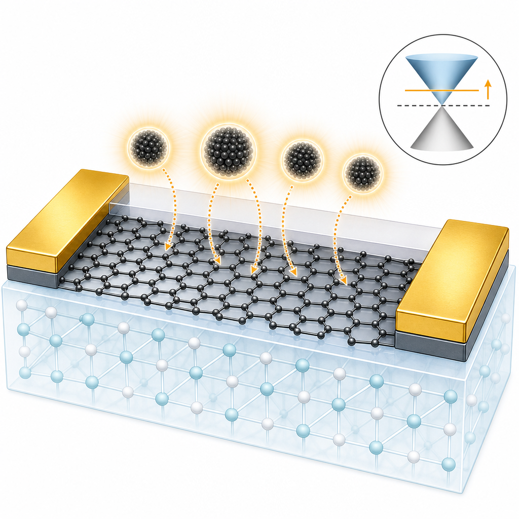
How ACS Material products were used
- CVD Graphene on Copper Foil (CVD Graphene) — “Monolayer graphene on copper foils was purchased from ACS Material or grown by chemical vapor deposition independently.”
Product Performance in this Study
The ACS Material monolayer graphene on copper foil served as the gate-tunable acceptor for resonant energy transfer from PbS quantum dots. After transfer to a LaF3 electrolyte gate, the graphene enabled ~50% photoluminescence modulation of individual quantum dots at room temperature and followed the expected 1/d^4 distance dependence.
Related product categories
Frequently asked questions
How does graphene switch quantum dot photoluminescence electrically?
Graphene acts as a tunable acceptor for resonant energy transfer from nearby quantum dots. Electrostatic gating shifts graphene's Fermi level; when |EF| exceeds half the emitter's exciton energy, the interband transition is blocked because the final state is filled or the initial state is depleted. Energy transfer is suppressed and the quantum dot recovers its radiative emission, producing a voltage-controlled on/off switch.
Why does energy transfer to graphene scale as 1/d^4 instead of the Forster 1/d^6?
Standard Forster theory treats two point dipoles, giving a 1/d^6 distance dependence. Graphene is a two-dimensional lossy medium, so the donor couples to a continuum of in-plane modes rather than a single acceptor dipole. Summing over those modes yields a 1/d^4 rate law that depends only on the donor-acceptor separation and universal constants such as the fine structure constant, independent of material specifics.
What grade of CVD graphene is suitable for hybrid quantum-emitter devices?
The experiment used commercial monolayer CVD graphene on copper foil with quality sufficient to support clean field-effect behavior under LaF3 electrolyte gating. After PMMA-assisted transfer, copper etching, and photolithography, the graphene served as a uniform 2D acceptor that produced the predicted d^-4 quenching and gate-tunable energy transfer, indicating that catalog-grade CVD monolayer graphene on Cu foil is suitable for such hybrid devices.