-
CVD Graphene Magnetic Superlattice - University of Illinois, 2024
Jun 09, 2026 | ACS MATERIAL LLCTosun, O. et al. (2024). Tunable magnetic confinement effect in a magnetic superlattice of graphene. *npj 2D Materials and Applications*. https://doi.org/10.1038/s41699-024-00468-7
npj 2D Materials and Applications · 2024
University of Illinois researchers use ACS Material CVD graphene on copper to build a Fe3O4 nanosphere magnetic superlattice with tunable Dirac points.
About this research
Researchers at the University of Illinois Urbana-Champaign used CVD monolayer graphene on copper foil purchased from ACS Material LLC to demonstrate a tunable magnetic superlattice in graphene, in which self-assembled Fe3O4 nanospheres imprint a periodic magnetic potential and produce superlattice Dirac points alongside a gapped energy spectrum near the K and K′ valleys. The work, published in npj 2D Materials and Applications (2024) by Tosun, Sarkar, Qian, Gilbert, Chen, and Mason, combines low-temperature transport, SQUID magnetometry, and self-consistent tight-binding calculations to show that quasiparticles are magnetically confined around the nanospheres and that an external field continuously tunes the superlattice response.
Band-structure engineering of two-dimensional materials is a central goal in condensed-matter physics, because periodic potentials can produce miniband formation, superlattice Dirac points, finite-energy chiral states, and even fractional Chern insulator behavior. Existing routes – moiré twisting, lithographic antidot patterning, and adatom deposition – are powerful but suffer from limited reproducibility, weak control of period and amplitude, or high fabrication cost. Klein tunneling also makes electrostatic confinement of Dirac fermions in graphene notoriously difficult, motivating the use of magnetic rather than electrostatic potentials. A scalable, field-tunable magnetic superlattice that operates on standard CVD graphene would open practical paths to engineered minibands, topological states, and quantum transport devices.
The device platform begins with monolayer graphene grown on 35-µm copper foil by chemical vapor deposition and supplied by ACS Material LLC. The team transferred the graphene to a 300 nm SiO2/Si back-gated substrate using a standard PMMA-supported wet transfer after etching the copper in 0.1 M ammonium persulfate. Electron-beam lithography and O2 reactive-ion etching defined a 6 µm × 1 µm Hall bar, followed by Ti(5 nm)/Au(20 nm) contacts. A windowed PMMA mask localized the deposition of 10.7 ± 0.7 nm Fe3O4 nanospheres, which self-assemble into hexagonal close-packed monolayer films spanning tens of micrometers. Forming-gas annealing at 300 °C for 30 minutes removed the oleic acid ligand shell so the nanospheres directly contacted the graphene. Transport was measured in a Quantum Design PPMS with a 9 T magnet using SR830 lock-in amplifiers, while magnetization was characterized with a Quantum Design MPMS3 SQUID.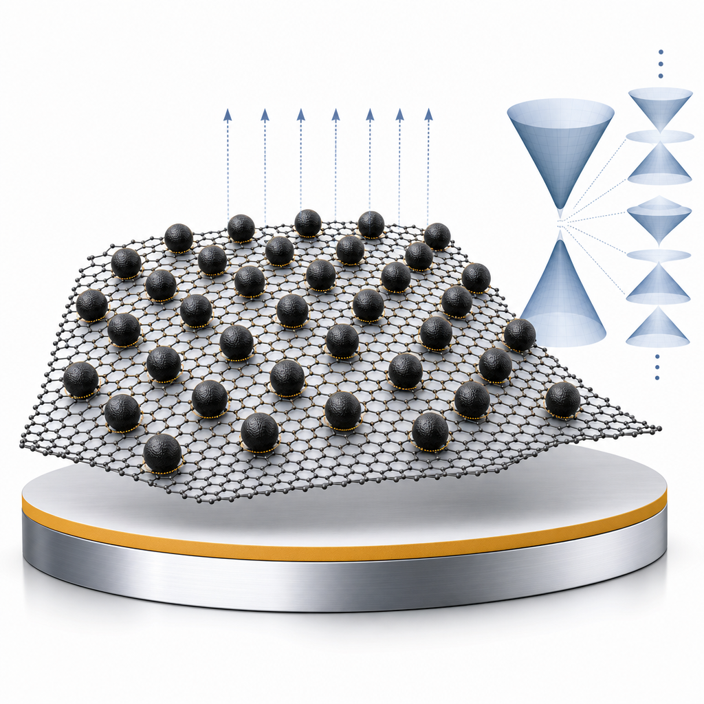
Key results center on three signatures of magnetic superlattice physics. First, the Fe3O4 nanospheres are superparamagnetic with a blocking temperature TB ≈ 50 K and become ferromagnetic below TB, producing a clear M–H hysteresis. The graphene/nanosphere stack shows non-metallic transport that follows a 2D variable-range hopping law, ln Rxx ∝ T^(−1/3), between 240 K and 50 K, with a deviation below TB consistent with closed-orbit confinement of carriers. Second, the device mobility at Vg = 0 V (n = 3.6 × 10^12 cm^−2) is 1155 cm^2 V^−1 s^−1, giving a mean free path of 26 nm and a phase coherence length of 91–112 nm, both larger than the 10–13 nm nanosphere period. The 2 K longitudinal resistivity shows nearly equally spaced gate-dependent dips with a periodicity of ΔV ≈ 1.4 V on both the electron and hole branches, identified by FFT analysis. Third, an external out-of-plane magnetic field tunes the superlattice: the FFT peak shifts to 3 V at 3 T and 7 T, then to 2.5 V at 9 T, while Landau levels at filling factors ν = 2 and ν = 6 emerge above 7 T. Quasi-periodic magnetoresistance oscillations between ±0.3 T and ±6 T match cyclotron orbits encircling integer numbers of nanospheres with a superlattice constant λ ≈ 12.6–13 nm, in agreement with SEM and TEM. Self-consistent tight-binding calculations with MNS = 0.2 eV reproduce both the superlattice Dirac points and the field-dependent density-of-states peaks.
This result is significant for several application areas. Magnetic-field-tunable superlattices on CVD graphene could underpin reconfigurable miniband electronics, valleytronic devices, and platforms for engineered topological states such as fractional Chern insulators. Because the superlattice is generated by self-assembled nanoparticles rather than e-beam patterning, the approach is scalable and applies to other 2D van der Waals and topological materials, including transition-metal dichalcogenides and magnetic vdW crystals. The authors point to follow-up work using angle-resolved photoemission spectroscopy to image the superlattice Dirac cones, and magnetic scanning gate microscopy to map proximity-induced magnetic domains in graphene.
For researchers building proximity-coupled 2D devices, the practical message is that wafer-scale CVD monolayer graphene on copper foil, like the material used here from ACS Material, is sufficient to host engineered superlattice physics when combined with controlled nanostructure assembly. The graphene catalog at ACS Material covers monolayer and multilayer CVD graphene on copper, SiO2, quartz, and PET, plus related 2D materials such as h-BN and TMDs, supporting groups working on band-structure engineering, spintronics, and quantum transport.How ACS Material products were used
- CVD Graphene on Copper Foil (CVD Graphene) — “Monolayer graphene, grown on 35 um thick copper foil using chemical vapor deposition, purchased from ACS Material LLC, was transferred onto SiO2 (300 nm)/Si substrates using standard wet transfer techniques.”
Product Performance in this StudyThe CVD monolayer graphene on copper foil from ACS Material served as the active 2D channel of the Hall bar device. After wet transfer to SiO2/Si, it supported the self-assembled Fe3O4 nanosphere superlattice and produced clear magnetic superlattice Dirac points and gate-dependent resistance oscillations, demonstrating that the graphene quality was sufficient (mobility ~1155 cm²/V·s, phase coherence length ~91-112 nm) to resolve the magnetic confinement physics.
Related product categories
Frequently asked questionsWhy use CVD graphene on copper for magnetic superlattice experiments?
CVD monolayer graphene on copper foil provides continuous, wafer-scale 2D channels that can be wet-transferred onto SiO2/Si back gates and patterned into Hall bars. In this study the graphene mobility of 1155 cm² V⁻¹ s⁻¹ and phase coherence length up to 112 nm were sufficient to resolve superlattice Dirac points and quasi-periodic magnetoresistance oscillations generated by a Fe3O4 nanosphere array with a 12–13 nm period.
How do Fe3O4 nanospheres modify the graphene band structure?
Below their 50 K blocking temperature the Fe3O4 nanospheres are ferromagnetic and imprint a periodic, radially inhomogeneous magnetic potential on the underlying graphene. This proximity-induced magnetism opens a gap near the K and K′ valleys and generates superlattice Dirac points, observed as gate-dependent resistance dips spaced by about 1.4 V at zero field, in agreement with self-consistent tight-binding calculations.
What role does the external magnetic field play in tuning the superlattice?
An out-of-plane magnetic field rotates the Fe3O4 magnetization vector out of the plane, which sharpens the magnetic potential and increases the gate-voltage period of the resistance dips from 1.4 V at 0 T to 3 V at 3–7 T. Above 7 T the field overwhelms the imprinted magnetism, Landau levels at filling factors ν = 2 and ν = 6 emerge, and the superlattice period contracts to 2.5 V at 9 T.