-
CVD Graphene Membranes for Molecular Sieving - MIT, 2012
May 28, 2026 | ACS MATERIAL LLCO’Hern, S. C. et al. (2012). Selective Molecular Transport through Intrinsic Defects in a Single Layer of CVD Graphene. *ACS Nano*. https://doi.org/10.1021/nn303869m
Massachusetts Institute of Technology · ACS Nano · 2012
MIT researchers used ACS Material CVD graphene on copper to build 25 mm² composite membranes showing size-selective molecular transport through intrinsic 1–15 nm pores.
About this research
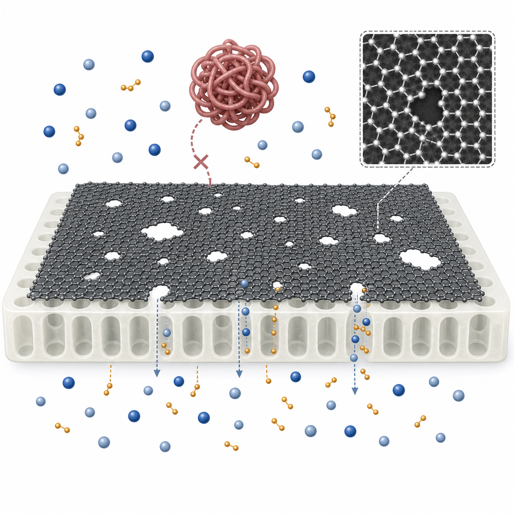
Researchers at the Massachusetts Institute of Technology used CVD graphene on copper foil purchased from ACS Material to construct large-area graphene composite membranes (GCMs) of more than 25 mm², and showed for the first time that single-layer CVD graphene exhibits size-selective molecular transport driven by intrinsic nanometer-scale pores. The team transferred the as-received graphene/copper foil onto a porous polycarbonate track-etch (PCTE) support, etched away the copper, and then measured both pressure-driven and diffusive transport of ions and molecules ranging from KCl to a 70 kDa tetramethylrhodamine dextran (TMRD). The graphene blocked the large dextran while permitting smaller species to cross, establishing a foundation for graphene-based separation membranes.
Nanoporous graphene has long been predicted to outperform conventional polymer membranes by orders of magnitude in both permeability and selectivity, with applications spanning water desalination, gas separation, and biomedical filtration. However, prior experimental work was limited to micrometer-scale suspended graphene patches, single nanopore DNA translocation devices, or graphene nanoballoon leak tests. Scaling selective transport measurements to macroscopic areas requires a route to suspend high-quality CVD graphene over porous supports without lithography or harsh solvents. The present study addresses that gap by combining a direct, polymer-conformal transfer technique with quantitative transport assays, and by linking the observed permeability to a measured pore-size distribution from aberration-corrected STEM imaging. The result clarifies how intrinsic defects, rather than handling damage, govern the molecular selectivity of large-area CVD graphene films.
The ACS Material product used was low-pressure CVD graphene grown on 25 μm copper foil, which the authors characterized by Raman spectroscopy before use. The graphene-on-copper sample was floated on APS-100 ammonium persulfate etchant to remove the backside graphene, rinsed, and then mechanically pressed against a non-PVP-coated, hydrophobic PCTE membrane with 200 nm cylindrical pores using a glass slide and a pipet-tube roller. Light finger pressure caused the pliable polycarbonate to conform to the contours of the copper and adhere to the graphene. The stack was then submerged in APS-100 under 7 psi gauge pressure for 5 minutes beyond full copper removal, rinsed in water followed by a 50% ethanol-water bath, and air-dried. The authors found that the hydrophobicity of the support, the surface roughness of the underlying copper (185 nm rms was used for final experiments versus 500 nm for earlier trials), and the use of ammonium persulfate rather than ferric chloride etchant were all critical to obtaining crack-free graphene over macroscopic areas.
SEM image analysis of the transferred GCMs showed graphene coverage of 90–98% across the 25 mm² area. Pressure-driven water flow measurements, which scale as D⁴/L through any uncovered 200 nm PCTE pores, independently confirmed effective coverages of 88–93% for three independent membranes (M1, M2, M3). Diffusive transport of 0.5 M KCl through these GCMs reached 46–71% of the bare PCTE flux, far higher than the ~10% expected if the graphene were impermeable, indicating that ions permeate the graphene through sub-50 nm openings. Diffusive selectivity emerged clearly when larger molecules were tested: the GCMs allowed transport of KCl (hydrated diameter ~0.66 nm), tetramethylammonium chloride (TMAC), and the 496 Da Allura Red AC dye (~1 nm), but reduced the diffusive flux of the 12 nm TMRD dextran by 80–85% relative to bare PCTE. Aberration-corrected STEM at 60 kV imaged intrinsic pores in the graphene lattice ranging from 1 to 15 nm in diameter, with roughly 83% of pores below 10 nm. A continuum diffusion model based on the measured pore-size distribution predicted graphene permeabilities consistent with experiment for a graphene porosity between 0.025% and 0.15%, supporting the interpretation that intrinsic CVD growth defects, rather than transfer-induced damage, drive the observed selectivity.
The demonstration that macroscopic CVD graphene films can serve as size-selective transport layers is directly relevant to next-generation membranes for water purification, desalination, gas separation, biomedical filtration, and dialysis. The authors specifically point to opportunities in controlling pore-size distribution and chemistry through optimized CVD growth, chemical treatment, or post-synthesis pore engineering, and they note that high-purity copper foils, smoother substrates, and tuned gas-flow conditions may further reduce intrinsic pore density. The PCTE-on-graphene composite architecture is also a model platform for evaluating any new 2D selective layer, and the diffusion-cell methodology established here has since become a standard tool in the graphene-membrane community. The work also informs the use of graphene as a barrier or corrosion-inhibiting film, where the same intrinsic defects limit performance.
For researchers building membranes, electrodes, or barrier films from large-area 2D materials, the ACS Material CVD Graphene on Copper Foil used here is available in the same form factor and provides a reproducible starting point. The category page (materials:cvd_graphene) lists this and related items, including graphene on SiO₂, quartz, PET, and TEM grids, supporting both transport studies and electronic device work. As shown in this study, careful characterization and transfer remain essential, and ACS Material's CVD graphene proved suitable for fabricating membranes over square-millimeter areas with quantifiable coverage and pore statistics.How ACS Material products were used
- CVD Graphene on Copper Foil (CVD Graphene) — “Low-pressure CVD graphene on 25 μm copper foil was purchased commercially from ACS Materials and characterized via Raman spectroscopy”
Product Performance in this Study
The ACS Material CVD graphene on 25 μm copper foil served as the active selective layer of the composite membrane. After transfer to a polycarbonate track-etch support, 90-98% coverage was achieved and the film exhibited size-selective molecular transport attributable to intrinsic 1-15 nm pores in the as-grown lattice.
Related product categories
Frequently asked questions
How does CVD graphene achieve size-selective molecular transport?
Single-layer CVD graphene contains intrinsic nanometer-scale pores formed during growth on copper. In this MIT study, aberration-corrected STEM revealed pores between 1 and 15 nm, with about 83% smaller than 10 nm. Small ions such as KCl and dye molecules near 1 nm pass through, while a 12 nm tetramethylrhodamine dextran is blocked, producing approximately 80–85% rejection compared to the bare polycarbonate support.
Why is ammonium persulfate preferred over ferric chloride for copper etching when transferring CVD graphene?
Ferric chloride (CE-100) produces poorly soluble copper(I) chloride crystals that nucleate on the graphene surface and mechanically tear the lattice along grain boundaries and wrinkles. Ammonium persulfate (APS-100) yields water-soluble copper(II) sulfate, leaving no crystal residues. The authors confirmed by SEM drop tests that APS-100 etching produces a clean graphene surface, enabling crack-free transfer over more than 25 mm² of polycarbonate track-etch membrane.
What graphene coverage can be achieved when transferring CVD graphene to a polycarbonate membrane?
Using direct pressing of CVD graphene on copper onto a non-PVP-coated polycarbonate track-etch membrane, followed by APS-100 etching under 7 psi, the MIT team achieved 90–98% coverage by SEM image analysis across approximately 25 mm². Independent pressure-driven water flow measurements gave coverages of 88–93% for three independently fabricated graphene composite membranes, confirming integrity after mounting in the diffusion cell.