-
CVD Graphene on Cu Foil for Low-Energy Electron PPM - Academia Sinica, 2017
Jun 22, 2026 | ACS MATERIAL LLCHsu, W. et al. (2017). Low-Energy electron point projection microscopy/Diffraction study of suspended graphene. *Applied Surface Science*. https://doi.org/10.1016/j.apsusc.2017.06.148
Applied Surface Science · 2017
Academia Sinica researchers use ACS Material CVD graphene on copper foil to study suspended graphene by low-energy electron point projection microscopy and diffraction.
About this research
Researchers at Academia Sinica, working with National Tsing Hua University, used ACS Material monolayer CVD graphene on copper foil to prepare suspended graphene membranes for a new low-energy electron point projection microscopy (PPM) and divergent-beam electron diffraction (DBED) instrument, reporting in Applied Surface Science (2017). The combined imaging/diffraction setup, built around a single-atom W(111) electron source operating at 40–500 eV, resolved individual adsorbates, identified graphene layer counts, and detected lattice ripples as small as 1 Å. The work establishes PPM/DBED as a low-cost, low-damage alternative to high-voltage TEM for studying suspended 2D materials.
Suspended graphene is the ideal support for imaging single molecules and biomolecules in electron microscopy because its atomic thickness, electrical conductivity, and high transparency minimize background. However, polymer-assisted transfers leave residues, and Raman spectroscopy is not sensitive to trace adsorbates. High-energy TEMs (100 keV) suffer from poor contrast on light atoms and induce beam damage; even 20–80 keV instruments cause chemical etching. A microscope that uses electrons below 500 eV offers very large scattering cross sections, ~26–27% opacity per graphene layer, and negligible knock-on damage, but requires clean, large-area suspended graphene to operate. Demonstrating such samples at wafer scale is therefore a prerequisite for the technique.
To prepare the suspended films, the authors transferred a CVD-grown graphene sheet from ACS Material, specified as "single layer graphene on a Cu foil, 4 inch × 2 inch," onto gold-coated Si3N4 membranes with periodic holes using a polymer-free transfer technique. The samples were annealed at 200 °C on a hot plate to remove moisture, and additional Joule heating in UHV (current ramped to 0.25 A at 0.02 A/min, held for ~12 h, reaching ~350 °C) was used to clean the surface. Raman spectroscopy confirmed the absence of the D peak around 1350 cm⁻¹, consistent with low-defect graphene. Imaging was performed in a UHV chamber at ~1 × 10⁻¹⁰ Torr, with a movable MCP/phosphor screen on a rail allowing the sample–screen distance D to vary from 30 mm to 132 mm—enabling both high-magnification PPM projections and high-angle DBED on the same area.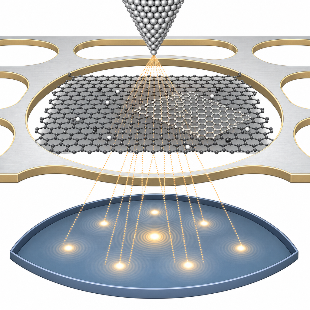
The ACS Material CVD graphene yielded large continuous suspended films spanning many membrane holes, with most regions showing single-layer transmission. After UHV annealing, sub-micron to over 1 μm wide regions of atomically clean graphene were obtained, against which individual adsorbates appeared as bright or dark spots with weak contrast and filament-like aggregates with apparent widths of ~10 nm. PPM/DBED clearly distinguished single-layer from double-layer regions (~750 nm wide double-layer ribbons rotated 23° relative to the underlying lattice were resolved). First-order diffraction disks revealed striped contrast patterns indicating both out-of-plane and in-plane ripples, with displacements estimated from a few angstroms up to the nanometer scale via the phase-shift relation φ = kh(1 − cos θ). The authors also documented an electron-dose effect: at small tip–sample separations (~1 μm) and high local current density, mobile hydrocarbon molecules ionized and aggregated, reducing total transmission by ~40% over 50 minutes. This finding is important because earlier PPM literature reported negligible beam effects.
The ability to image suspended graphene with low-energy electrons supports several applications: characterization of 2D material heterostructures and grain boundaries, evaluation of cleanliness for van der Waals stacking in energy storage and optoelectronics, and ultimately coherent diffractive imaging (CDI) of single organic or biological molecules adsorbed on graphene. The paper outlines next steps toward lensless CDI, including smaller Si3N4 holes to satisfy the oversampling requirement, cryogenic operation to immobilize adsorbates and reduce contamination, and a complementary proximity STEM mode operating between PPM and STM regimes at 5–40 eV for thicker samples.
For researchers working on suspended 2D membranes, TEM grid supports, or low-voltage electron imaging, CVD graphene on copper foil from ACS Material is available in sizes suitable for transfer onto perforated Si3N4 or TEM grids. The same monolayer film grade was used as a polymer-free transferred support in this study and proved compatible with UHV annealing protocols and electron-beam imaging at 40–500 eV.How ACS Material products were used
- CVD Graphene on Copper Foil (CVD Graphene) — “we transferred a CVD-grown graphene sheet (ACS material, single layer graphene on a Cu foil, 4 inch × 2 inch) onto the Si3N4 membranes using a polymer-free transfer technique”
Product Performance in this StudyThe ACS Material monolayer CVD graphene on copper foil was successfully transferred polymer-free onto perforated Si3N4 membranes, producing large-area suspended single-layer graphene that supported low-energy electron point projection microscopy/diffraction studies. After UHV annealing, sub-micron to micron-scale clean regions were achieved, enabling clear imaging of adsorbates, ripples, and grain orientations.
Related product categories
Frequently asked questionsWhy use CVD graphene on copper foil as a support for low-energy electron microscopy?
CVD graphene on copper foil provides large-area, continuous monolayer films that can be transferred onto perforated Si3N4 membranes to create wafer-scale suspended graphene. Its atomic thickness gives roughly 26–27% opacity per layer to 40–500 eV electrons, producing strong contrast while remaining largely transparent. The film tolerates UHV annealing to remove polymer residues and adsorbates, yielding micron-scale clean regions essential for imaging single molecules and lattice ripples.
How does point projection microscopy reveal graphene ripples that TEM may miss?
Point projection microscopy projects field-emitted low-energy electrons from a single-atom tip onto a movable screen, allowing simultaneous projection imaging and high-angle divergent-beam diffraction. Out-of-plane ripples produce a scattering phase shift φ = kh(1 − cos θ) that grows with scattering angle, so even angstrom-scale corrugations invisible in the zero-order spot create strong striped contrast in first- and higher-order diffraction disks. This sensitivity to sub-nanometer height variation surpasses conventional zero-order TEM imaging.
What causes adsorbate aggregation on suspended graphene under a low-energy electron beam?
At small tip-to-sample separations of about one micrometer, the local current density rises sharply. Around 100 eV, electron impact ionization of hydrocarbon molecules such as CH4 is near maximum, so mobile residual hydrocarbons on the graphene can be ionized, polymerize, and bond to existing filament-like aggregates. The authors observed total transmission dropping by about 40% over 50 minutes, indicating that long-duration high-dose imaging, not residual gas adsorption alone, drives the buildup.