-
CVD Graphene on SERS Metasurfaces - Stanford University, 2019
Jun 19, 2026 | ACS MATERIAL LLCThareja, V. et al. (2019). Anisotropic metasurfaces as tunable SERS substrates for 2D materials. *ACS Photonics*. https://doi.org/10.1021/acsphotonics.9b00416
Stanford University · ACS Photonics · 2019
Stanford researchers use CVD graphene from ACS Material on anisotropic gold metasurfaces, achieving 25× G-peak and 50× 2D-peak Raman enhancement.
About this research
Researchers at Stanford University demonstrated that anisotropic gold metasurfaces patterned with subwavelength grooves can act as tunable surface-enhanced Raman scattering (SERS) substrates for two-dimensional materials, achieving up to 25× enhancement of the graphene G-peak and 50× enhancement of the 2D-peak using single-layer CVD graphene supplied by ACS Material. Published in ACS Photonics (2019) by Thareja, Esfandyarpour, Kik, and Brongersma, the paper shows that the engineered direction and magnitude of the near-surface electric field can be used to read out the Raman polarizability tensor of an atomically thin material. The same metasurface geometry can also suppress Raman peaks by 40% at specific groove dimensions, opening a route to controllable background reduction in SERS spectra.
Conventional SERS substrates—roughened silver films, colloidal aggregates, and randomly distributed plasmonic nanoparticles—deliver strong but irreproducible enhancements because their hot spots depend sensitively on surface topography, and they offer little control over the direction of the local electric field. This is a long-standing obstacle for studying anisotropic vibrational modes in 2D materials such as graphene and transition metal dichalcogenides, where the symmetry of the Raman tensor carries information about phonon character, strain, and orientation. A SERS substrate that produces reproducible, vector-controlled near-field enhancements would let researchers separate the contributions of differently polarized Raman dipoles and quantify the symmetry of bond vibrations. The Stanford team approached this problem by replacing roughened plasmonic surfaces with deterministic metasurfaces, where the field at the surface is governed by gap-plasmon resonances inside engineered grooves rather than by uncontrolled localized hot spots.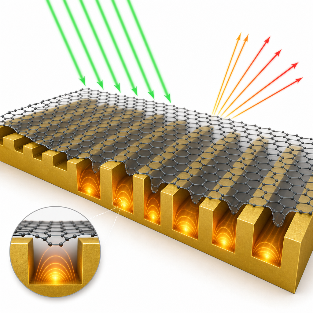
In the experimental workflow, an optically thick (~275 nm) Au film was deposited by electron-beam evaporation on a 300 nm SiO2/Si wafer. Linear groove arrays were then milled into the gold using a FEI Helios focused ion beam, with a fixed periodicity of 200 nm and groove widths of 75, 95, and 170 nm; groove depths were varied in thirteen steps from 30 to 210 nm, yielding 39 distinct 5 × 5 µm² metasurfaces on a single substrate. Single-layer CVD graphene obtained from ACS Material was then transferred directly onto the patterned gold surface, providing a uniform, atomically thin Raman probe layer placed at the location of the engineered field maximum. The graphene-coated metasurfaces were illuminated at near-normal incidence with a 532 nm laser through a 20×, 0.4 N.A. objective on a Witec Alpha 500 confocal Raman system. Twenty-five spectra were collected on each patterned region and on adjacent unpatterned gold to give a Normalized Raman Enhancement (NRE). Quality and continuity of the as-transferred CVD graphene were essential, since defects or wrinkles would have masked the geometry-dependent trends the authors set out to measure.
For optimized 75-nm-wide, ~70-nm-deep grooves the graphene G-peak (581 nm under 532 nm excitation) was enhanced ~25× and the 2D-peak (621 nm) ~50× relative to an as-deposited gold film. The factor-of-two difference between the two peaks directly reflects the anisotropic Raman polarizability of graphene: the G-peak (E2g symmetry) produces Raman dipoles both along and across the grooves, but only the cross-groove component couples to the gap-plasmon resonance, while the 2D-peak (A1g-symmetric, radial breathing) emits a Raman dipole aligned with the pump polarization perpendicular to the grooves and thus enjoys the full collection enhancement. As groove depth was swept, NRE values traced a clear resonance peaking near d ≈ λ0/4nSPP and shifted to deeper grooves as groove width increased, in agreement with FDTD simulations using a Kubo-formalism graphene layer and an ~6 nm air gap. At groove depths near 178 nm the NRE fell to ~0.6, demonstrating a controllable ~40% suppression of the Raman signal—useful for masking background in areas outside a region of interest. Reflectance minima red-shifted with groove depth, confirming the spectral tunability of the gap-plasmon resonance.
The approach is broadly applicable to optical and vibrational studies of 2D semiconductors, ultrathin films, and adsorbed molecules. Because the field enhancement is governed by engineered geometry rather than random roughness, these metasurfaces provide a reproducible platform for polarization-resolved SERS, phonon-symmetry analysis in transition metal dichalcogenides, and orientation studies of molecules deposited on top of a 2D spacer layer. Applications include trace chemical sensing with reduced substrate background, biosensing on graphene-functionalized SERS chips, and fundamental studies of light–matter interaction in van der Waals materials. The work also points toward integrating tunable metasurface SERS substrates into wafer-scale platforms compatible with CVD-grown 2D materials.
For researchers planning similar polarization-resolved SERS or 2D-material plasmonics experiments, the study illustrates that consistent, transferable monolayer graphene is critical: small variations in coverage or contamination translate into large changes in the measured enhancement factor. CVD graphene of the type used here is available from ACS Material in formats suitable for transfer onto pre-patterned plasmonic substrates, supporting reproducible work on tunable SERS, Raman tensor analysis, and vibrational spectroscopy of 2D layers.How ACS Material products were used
- CVD Graphene (single-layer, transferable) (CVD Graphene) — “Commercially available CVD graphene (from ACS Material) is then transferred onto the fabricated metasurfaces.”
Product Performance in this StudySingle-layer CVD graphene from ACS Material served as the 2D test material whose Raman G- and 2D-peak intensities were probed against the metasurface. The high-quality, large-area transferable monolayer enabled reproducible Raman measurements showing 25× (G-peak) and 50× (2D-peak) signal enhancement and ~40% suppression at tuned groove dimensions.
Related product categories
Frequently asked questionsHow does an anisotropic metasurface enhance graphene's Raman signal?
Subwavelength grooves milled into a gold film support gap-plasmon resonances that concentrate the incident field at the surface where the graphene sits. When the groove depth approaches a quarter of the gap-plasmon wavelength, the field at the metasurface reaches several times the incident value, and this enhancement multiplies in both excitation and collection, producing roughly 25× enhancement for graphene's G-peak and 50× for the 2D-peak.
Why are the G-peak and 2D-peak enhanced by different amounts on the same metasurface?
The difference reflects graphene's anisotropic Raman polarizability tensor. The G-peak (E2g symmetry) produces Raman dipoles both along and across the grooves, but only the dipole perpendicular to the grooves couples efficiently to the gap-plasmon resonance. The 2D-peak (A1g symmetry) emits a Raman dipole aligned with the pump polarization perpendicular to the grooves, so it benefits fully from the collection enhancement, giving roughly twice the enhancement of the G-peak.
What grade of CVD graphene is suitable for plasmonic SERS substrates?
Continuous, large-area single-layer CVD graphene that can be cleanly transferred onto patterned plasmonic substrates is preferred. The Stanford study used transferable monolayer CVD graphene from ACS Material, which sits directly on the metasurface with only a few nanometers of effective spacing. Uniform coverage and low defect density are important because residues or holes mask the geometry-dependent Raman trends used to read out the polarizability tensor.