-
CVD Graphene Photodetector with Pt Nanoparticles - Zhejiang University, 2018
Jun 16, 2026 | ACS MATERIAL LLCHuang, K. et al. (2018). High and fast response of a graphene–silicon photodetector coupled with 2D fractal platinum nanoparticles. *Advanced Optical Materials*. https://doi.org/10.1002/adom.201700793
State Key Laboratory of Silicon Materials and School of Materials Science and Engineering Zhejiang University Hangzhou Zhejiang 310027 China · Advanced Optical Materials · 2018
Zhejiang University coupled ACS Material CVD graphene with 2D fractal Pt nanoparticles to build a Gr–Si photodetector with 26 A/W responsivity and 78 ns response.
About this research
Researchers at State Key Laboratory of Silicon Materials and School of Materials Science and Engineering Zhejiang University Hangzhou Zhejiang 310027 China used commercial single-layer CVD graphene purchased from ACS Material to fabricate a graphene–silicon (Gr–Si) Schottky photodetector that, when coupled with 2D fractal platinum nanoparticles, reaches a responsivity of 26 A W⁻¹, a fast 78 ns response time, and a noise-equivalent power as low as 4.2 pW Hz⁻⁰·⁵ in the visible range. The work demonstrates that combining plasmonic absorption enhancement with physical doping of graphene by a high-work-function metal can simultaneously boost photoresponse and increase device speed.
Graphene–silicon Schottky photodetectors are attractive because the Gr/Si junction is electrically simple, scalable, and naturally fast. However, the low work function of pristine graphene gives a small Schottky barrier, and graphene alone absorbs only a few percent of incident light, so practical Gr–Si photodetectors suffer from poor responsivity and high background noise. Chemical doping can raise the work function but tends to be unstable and can damage graphene. Plasmonic metal nanoparticles offer an alternative, but they typically agglomerate or require expensive lift-off lithography to form fractal metasurfaces. The paper addresses this gap by introducing solution-synthesized 2D fractal Pt nanoparticles that combine the optical benefits of a fractal metasurface with simple drop-coating processing onto a graphene electrode supplied by ACS Material.
The ACS Material single-layer CVD graphene is the device-defining active layer. As described in the experimental section, the team "fabricated by using commercial single-layer Gr (bought from ACS Material) and n-type <100> Si wafers (1–10 ohm cm)." A PMMA-based wet transfer process was used: PMMA was spin-coated onto the as-grown graphene, ammonium persulfate etched the copper growth substrate, and the floating Gr/PMMA film was rinsed in deionized water before being placed onto HF-treated Si wafers. The stack was then annealed at 400 °C in argon inside a tube furnace to vaporize the PMMA and improve the Gr/Si interface. Silver served as the front contact and In–Ga alloy as the back contact. After Gr/Si fabrication, an oleic-acid-in-water emulsion synthesis (with H₂PtCl₆ and NaBH₄ in the presence of Pluronic F127) produced quasi-2D fractal Pt nanoparticles ~30 nm in diameter with ~5 nm branch widths, which were then spin- or drop-coated onto the graphene to form a uniform ~15 nm-thick film. The quality of the underlying CVD graphene directly governs Schottky barrier reproducibility and dark current, making the ACS Material film central to the result.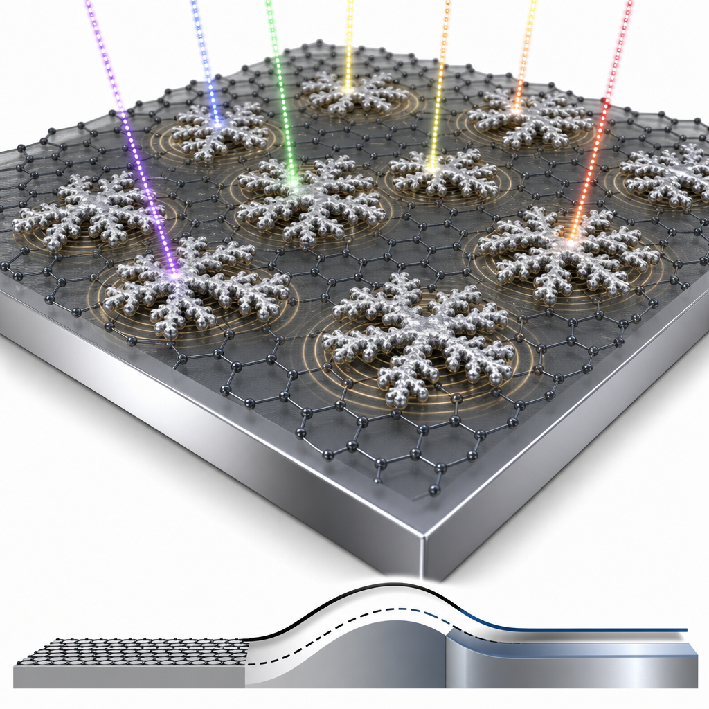
The quantitative results highlight the benefit of pairing high-quality CVD graphene with the fractal Pt nanoparticles. The maximum responsivity reaches 26 A W⁻¹, which the authors state is the best reported for Gr–Si photodetectors of this geometry at the time of publication. Incident photon conversion efficiency (IPCE) rises above 81% across the visible range, an improvement of about 30% over the pristine Gr/Si device, while the calculated internal quantum efficiency exceeds 99%, indicating that essentially all absorption gain is converted to photocurrent. Reflectance drops to roughly one third of the pristine value. Ultraviolet photoelectron spectroscopy shows that the Pt nanoparticles increase graphene's work function by 0.1 eV, and current–voltage analysis yields a 16 meV rise in the Schottky barrier height. The strengthened built-in field accelerates carrier separation, giving a 78 ns switch-on time, and suppresses recombination-driven diffusion noise, dropping NEP from 15.5 pW Hz⁻⁰·⁵ to 4.2 pW Hz⁻⁰·⁵. The specific detectivity reaches 7.5 × 10¹⁰ Jones under AM 1.5 illumination. Even at incident powers as low as 5 µW cm⁻², the fractal-Pt device produced a measurable photocurrent, whereas the pristine device did not.
The combination of high responsivity, fast switching, and low noise positions this Gr–Si platform for dim-light visible photodetection, low-light imaging arrays, and integrated silicon photonic receivers. The fractal-nanoparticle strategy is also adaptable: morphology can be tuned via the emulsion synthesis to target different spectral regions or different 2D-material absorbers, and the same physical-doping concept could be applied to graphene–GaAs, graphene–GaN, or transition-metal-dichalcogenide heterojunctions. The authors point out that this hybrid plasmonic/Schottky strategy avoids the storage instability of chemical dopants and the cost of lift-off metasurface lithography, which should aid practical deployment in CMOS-compatible photodetector arrays.
For researchers reproducing or extending this work, the device performance depends strongly on the quality and uniformity of the starting CVD graphene. ACS Material's single-layer CVD graphene on copper foil, used here as the active layer, is part of the company's CVD Graphene catalog and is available to groups working on Schottky photodetectors, transparent electrodes, and plasmonic 2D-material hybrids. The product enabled a clean PMMA transfer onto HF-treated Si and a reproducible Gr/Si junction, which is a prerequisite for the modest 16 meV barrier shift and the resulting noise reduction to be observable.How ACS Material products were used
- CVD Graphene on Copper Foil (single-layer) (CVD Graphene) — “The Gr–Si detectors were fabricated by using commercial single-layer Gr (bought from ACS Material) and n-type <100> Si wafers (1–10 ohm cm).”
Product Performance in this StudyThe ACS Material single-layer CVD graphene served as the Schottky-junction electrode on n-Si. After PMMA-assisted transfer and annealing, it formed a high-quality Gr/Si interface that, combined with fractal Pt nanoparticles, delivered 26 A W⁻¹ responsivity and 78 ns response.
Related product categories
Frequently asked questionsHow do fractal platinum nanoparticles improve a graphene–silicon photodetector?
Fractal Pt nanoparticles act simultaneously as a plasmonic absorber and a p-type dopant for graphene. Their highly curved 2D branches concentrate the local electric field about five times above background, scattering more light into the silicon and raising IPCE above 81%. Because Pt's work function is ~5.7 eV, holes transfer into graphene, lifting its work function by 0.1 eV and increasing the Schottky barrier by 16 meV, which lowers noise and speeds response.
Why is CVD graphene preferred as the Schottky electrode in Gr–Si photodetectors?
CVD graphene provides large-area, continuous monolayer films that can be transferred onto silicon to form a uniform Schottky junction. Wafer-scale CVD material, such as the single-layer graphene on copper foil supplied by ACS Material, gives reproducible work functions and low pinhole density, both of which are critical for low dark current and consistent barrier height. It is also compatible with standard PMMA-assisted transfer and post-anneal cleanup at 400 °C in argon.
What responsivity and response time can a Pt-decorated graphene–silicon photodetector achieve?
In this work the Pt-fractal/Gr–Si photodetector reached 26 A W⁻¹ responsivity, a 78 ns switching response, and a noise-equivalent power of 4.2 pW Hz⁻⁰·⁵ in the visible range, with a specific detectivity of 7.5 × 10¹⁰ Jones under AM 1.5 illumination. These numbers place the device above earlier Gr–Si detectors of comparable geometry, particularly under dim-light conditions below 50 µW cm⁻².