-
CVD Graphene Photodetectors with Si3N4 - Beijing Jiaotong, 2018
Jun 22, 2026 | ACS MATERIAL LLCSu, F. et al. (2018). Long-term stability of photodetectors based on graphene field-effect transistors encapsulated with Si3N4 layers. *Applied Surface Science*.
Applied Surface Science · 2018
Beijing Jiaotong University built Si3N4-encapsulated graphene FET photodetectors on ACS Material CVD graphene, reaching 6.3 mA/W and 2-month air stability.
About this research
Researchers at Beijing Jiaotong University, together with collaborators at the Institute of Microelectronics of the Chinese Academy of Sciences (IMECAS), used monolayer CVD graphene supplied by ACS Material, LLC to build buried-gate graphene field-effect transistor (GFET) photodetectors and demonstrated that a PECVD Si3N4 encapsulation layer delivers long-term air stability while raising photoresponsivity to 6.3 mA/W at 785 nm under a gate bias of only 6 V. Published in Applied Surface Science (2018), the work shows that simple Si3N4 capping can simultaneously protect graphene from atmospheric doping, induce useful n-type doping, and outperform conventional back-gated graphene photodetectors that normally require gate voltages up to 80 V.
Graphene's gapless band structure, ultrafast carrier dynamics, and broadband absorption from ultraviolet to terahertz make it one of the most attractive active materials for photodetectors. However, open-face graphene devices are notoriously sensitive to H2O, O2, and airborne contamination, all of which produce uncontrolled p-type doping and steady drift of electrical resistance. For graphene photodetectors to leave the lab and reach real applications such as optical communication, imaging, and on-chip sensing, the active channel must be isolated from the ambient environment. The authors target this practical bottleneck and benchmark Si3N4 against alternative encapsulants (Ti, pentacene, self-assembled monolayers, Al2O3, h-BN), noting that Si3N4 combines broad optical transparency, chemical and mechanical robustness, and full compatibility with standard integrated-circuit fabrication.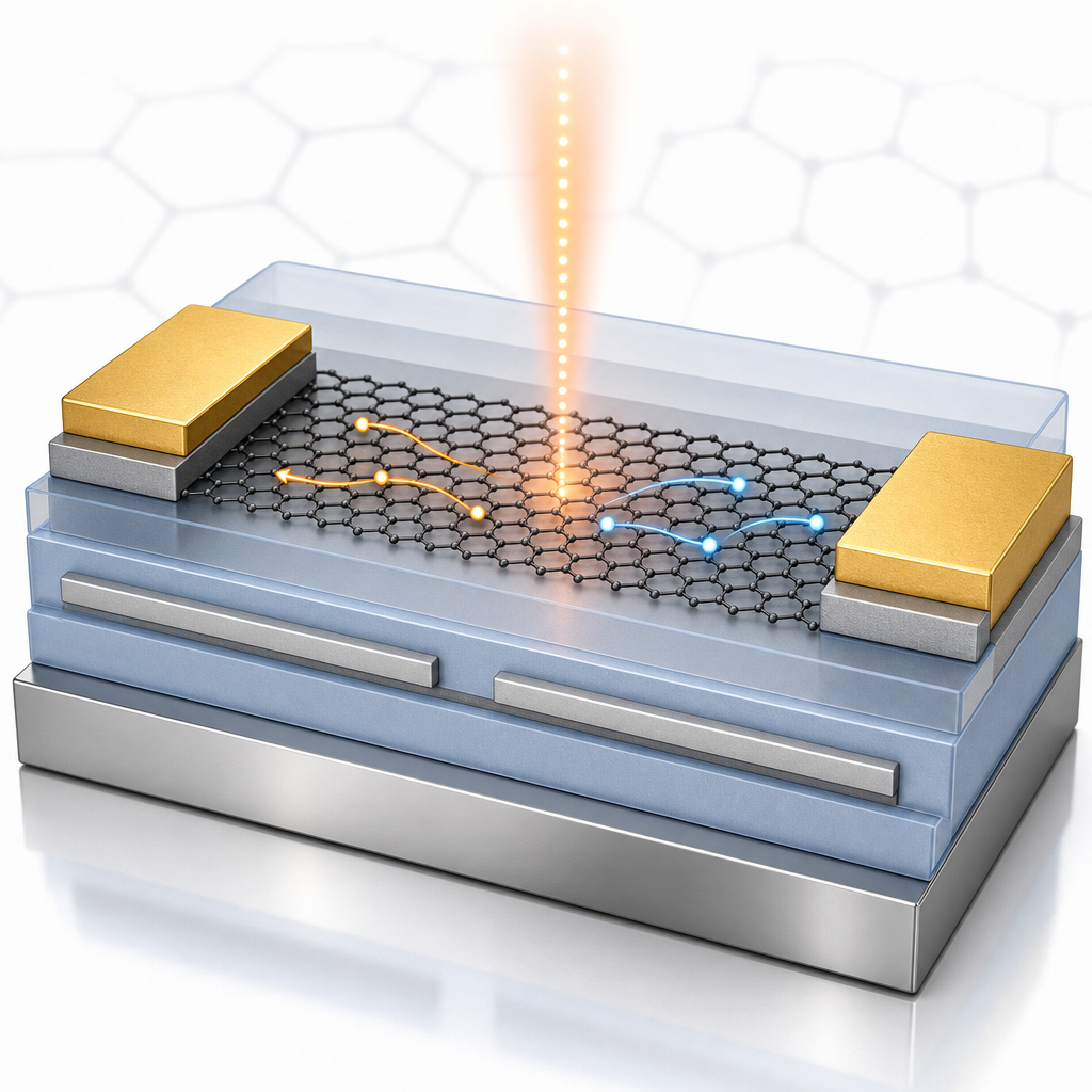
Monolayer CVD graphene from ACS Material was the active channel of every device. The fabrication flow began with a 200 nm PECVD Si3N4 bottom protective layer on a silicon wafer, followed by sputtered Cr/Pt buried gate electrodes (10 nm/50 nm) and a 30 nm PECVD SiO2 gate dielectric. The ACS Material CVD graphene was then transferred onto the SiO2 surface and patterned by oxygen plasma etching to define 30 µm × 100 µm and 14 µm-long conductive channels. Cr/Au (10 nm/50 nm) source and drain electrodes were deposited by electron beam evaporation, yielding open-face GFETs as reference devices. A 30 nm top Si3N4 layer was finally deposited by PECVD to encapsulate the channel. Raman spectroscopy confirmed monolayer character of the ACS Material graphene, with characteristic G (~1582 cm⁻¹) and 2D (~2683 cm⁻¹) peaks; after Si3N4 deposition both peaks downshifted (ΔG = −3.9 cm⁻¹, Δ2D = −10.6 cm⁻¹), consistent with reduced p-type doping and additional n-type doping at the graphene/Si3N4 interface.
Electrically, the open-face reference GFETs showed ambipolar transfer characteristics with the Dirac point at +11.7 V (strongly p-doped by adsorbed H2O and O2), a contact resistance of 435 Ω, and an intrinsic field-effect mobility of 1010 cm²/(V·s). Encapsulation with 30 nm Si3N4 shifted the Dirac point down to +8.9 V, confirming n-type doping, while contact resistance rose to 1736 Ω and hole mobility decreased to 698 cm²/(V·s) due to encapsulation-induced disorder. Under 514 nm laser illumination at zero gate and drain bias, the encapsulated devices exhibited reproducible on/off photocurrent cycling and a photoresponsivity of 6.3 µA/W that rose linearly with optical power. Tuning the gate bias drove the photoresponsivity up to 1.0 mA/W at Vg = −2 V (514 nm), 1.2 mA/W at 633 nm, and a peak of 6.3 mA/W at 785 nm—more than four times higher than typical back-gated GFET photodetectors (~1.5 mA/W) and approaching suspended GFET values (~10 mA/W), all achieved at gate biases below 6 V instead of 80 V. After two months of ambient exposure (20–25 °C, 40–60% relative humidity), the encapsulated GFETs drifted only 11.6% in resistance, while the open-face controls drifted by 129.8%.
The demonstrated combination of low operating voltage, broadband response from 514 to 785 nm, and multi-month air stability is directly relevant to silicon-photonics-integrated graphene photodetectors, optical interconnects, on-chip spectroscopy, and wearable optoelectronics. Because PECVD Si3N4 deposition is a standard back-end step in CMOS foundries, the approach can be ported with little change to other emerging 2D photoactive materials, including MoS2, WS2, SnS2, SnSe, and V2O5, where ambient instability is similarly limiting. The authors specifically suggest that introducing a high-temperature vacuum pre-bake (as reported for MoS2 transistors) could further suppress Coulomb scattering and recover the contact resistance and mobility lost during encapsulation, providing a clear path to next-generation devices.
For researchers building photodetectors, transistors, or sensors that depend on a clean, reproducible monolayer carbon channel, the quality of the starting CVD graphene determines the entire device performance envelope. ACS Material's CVD Graphene on Copper Foil—the product used in this study—is available in monolayer form suitable for transfer onto SiO2, quartz, PET, or custom substrates and is well-matched to the buried-gate GFET workflow demonstrated here. Groups working on Si3N4-passivated 2D devices, graphene electro-optic modulators, or air-stable flexible electronics can adopt the same source material to reproduce and extend these results.How ACS Material products were used
- CVD Graphene on Copper Foil (CVD Graphene) — “monolayer CVD-grown graphene (ACS Material, LLC) was transferred onto the SiO2 layer and patterned using oxygen plasma etching”
Product Performance in this StudyThe CVD-grown monolayer graphene served as the photoactive conductive channel of the buried-gate field-effect transistor. Raman spectra confirmed monolayer character with clear G and 2D peaks, and the resulting devices delivered a hole mobility of 1010 cm²/(V·s) before encapsulation and a photoresponsivity of 6.3 mA/W at 785 nm after Si3N4 encapsulation.
Related product categories
Frequently asked questionsHow does Si3N4 encapsulation improve graphene photodetector stability?
A PECVD Si3N4 layer blocks H2O, O2, and airborne contaminants from reaching the graphene channel, preventing the uncontrolled p-type doping and resistance drift that plague open-face devices. In this study a 30 nm Si3N4 cap held the GFET resistance change to 11.6% over two months in ambient air, while unencapsulated reference devices drifted by 129.8% over the same period.
Why use CVD graphene for buried-gate field-effect transistor photodetectors?
Buried-gate GFET photodetectors require a continuous, uniform monolayer of graphene that can be patterned into micrometer-scale channels. Monolayer CVD graphene grown on copper foil meets these needs because it can be transferred onto SiO2 dielectrics, etched by oxygen plasma into defined geometries, and contacted by evaporated Cr/Au electrodes, yielding ambipolar transfer characteristics and field-effect mobilities above 1000 cm²/(V·s).
What photoresponsivity can a Si3N4-encapsulated graphene FET photodetector reach?
The encapsulated devices reached 6.3 mA/W at 785 nm, 1.2 mA/W at 633 nm, and 1.0 mA/W at 514 nm under zero source-drain bias and gate biases below 6 V. This 785 nm value is more than four times higher than typical back-gated GFET photodetectors that often require gate voltages up to 80 V, and approaches the responsivity of suspended graphene photodetectors.