-
CVD Graphene Salisbury Screen Absorber - Stanford, 2015
Jun 12, 2026 | ACS MATERIAL LLCThareja, V. et al. (2015). Electrically tunable coherent optical absorption in graphene with ion gel. *Nano Letters*. https://doi.org/10.1021/nl503431d
Stanford University · Nano Letters · 2015
Stanford researchers use ACS Material CVD graphene in an ion-gel-gated Salisbury screen to achieve 3.3% per volt mid-IR absorption modulation.
About this research
Researchers at Stanford University demonstrated electrically tunable coherent optical absorption in a single sheet of CVD graphene from ACS Material, integrated into an ion-gel-gated Salisbury screen that modulates mid-infrared light at 3.3% per volt. The device places one layer of graphene above a 600 nm silica spacer and a 200 nm gold back reflector, then gates the graphene through a 4.5 µm ionic gel derived from DEME-TFSI. Reported in Nano Letters (2015) by Thareja and coworkers in the Brongersma group, the work establishes a low-voltage route to large optical modulation in atomically thin films and reveals an unexpected coherent absorption boost contributed by the ion gel itself.
Dynamic control of light absorption in two-dimensional materials is a central challenge for infrared modulators, photodetectors, and thermal emitters. A pristine single graphene layer absorbs only about 2.3% of incident light, which is too weak for practical optoelectronic devices, and conventional back-gate dielectrics such as Si3N4 require tens of volts to shift the Fermi level meaningfully. Plasmonic patterning, waveguide integration, and high-Q microcavities have all been pursued to enhance graphene absorption, but each adds fabrication complexity or restricts operation bandwidth. A Salisbury screen geometry, in which an absorber is placed roughly a quarter wavelength above a metallic mirror, offers a simpler path to constructive field enhancement at the absorber plane, and combining it with low-voltage ionic gating opens a regime of efficient mid-IR modulation directly relevant to vibrational spectroscopy and infrared sensing.
The ACS Material CVD graphene was the atomically thin active layer of the device. The authors state explicitly that "commercially available CVD graphene (from ACS Material) was then transferred onto the SiO2 spacer." The full stack was built on a silicon substrate: e-beam evaporation of the 200 nm gold back reflector, HDPECVD growth of a 600 nm SiO2 spacer designed to place a standing-wave antinode at the graphene plane near 3.2 µm, transfer of the CVD graphene, and patterning of gold source, drain, and lateral gate pads. A 4.5 µm ionic gel layer derived from the ionic liquid DEME-TFSI was then spin-coated to provide top gating. With this layout, charge accumulation at the gel/graphene and gel/Au electric double layers tunes the graphene Fermi level over hundreds of meV at only a few volts, allowing in-situ FTIR reflectance measurements as a function of bias.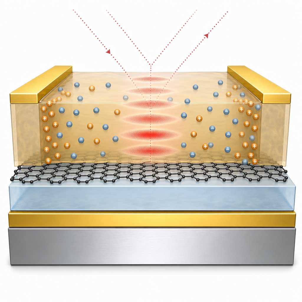
Drain-source transport showed a clear charge neutrality point at a gate bias of 0.8 V, indicating that the as-transferred graphene was slightly p-doped. Using an estimated double-layer capacitance of 1.45 × 10⁻³ F/m², gate voltages of 0.8, 1.8, 2.0, and 2.6 V correspond to Fermi level positions of 0, 0.13, 0.16, and 0.195 eV. Reflectance spectra modeled with a Fresnel transfer matrix and a Kubo-formula conductivity matched the FTIR data well across four Fabry-Pérot-like resonances near 2.7, 3.2, 4.2, and 5.8 µm. The graphene plane experiences an approximately doubled electric field amplitude at the design wavelength, quadrupling the absorption relative to a suspended sheet. The finite-thickness ionic gel adds a second weakly reflecting interface (Fresnel coefficient ≈ 0.17 at the gel/air boundary), and constructive interference of this contribution raises the absorption enhancement to about 5.5× over suspended graphene, a 40% boost beyond a basic Salisbury screen. The measured electrically induced absorption modulation reaches 3.3% per volt, the highest reported in any atomically thin active layer at that time, with absorption losses in the gold mirror staying below 2% and varying by only ~0.06% across the bias range.
This architecture is directly relevant to mid-infrared electro-optic modulators, tunable thermal emitters and absorbers, IR vibrational spectroscopy, gas and chemical sensing, and active metasurfaces. The authors note that combining higher-mobility graphene with plasmonic patterning into nanoscale resonators could push absorption modulation well beyond 10%, and that ionic-gel gating provides a path to low-voltage operation otherwise impossible with thick back-gate dielectrics. The work also contributes to the broader effort of engineering coherent absorption in two-dimensional solids and metasurfaces, where the interplay between standing-wave field profiles and tunable conductivity dictates device performance.
For researchers pursuing similar tunable two-dimensional photonic devices, large-area CVD graphene of the kind used in this study is available from ACS Material as CVD Graphene on Copper Foil and related transfer-ready formats. The product enabled wafer-scale integration onto an oxide/metal stack without compromising the optical and electrical quality required to resolve subtle coherent absorption effects, and is suitable for groups building infrared modulators, electro-optic test structures, and gated 2D heterostructures.How ACS Material products were used
- CVD Graphene on Copper Foil (CVD Graphene) — “Commercially available CVD graphene (from ACS Material) was then transferred onto the SiO2 spacer.”
Product Performance in this StudyThe CVD graphene from ACS Material served as the atomically thin absorbing layer in the Salisbury screen, enabling a record electrical absorption modulation of 3.3% per volt and up to 5.5× absorption enhancement over a suspended graphene sheet.
Related product categories
Frequently asked questionsHow does an ion gel improve electrical gating of graphene compared to conventional back-gate dielectrics?
Ion gels form electric double layers only a few nanometers thick at the gel/graphene interface, giving a very large specific capacitance (about 1.45 mF/m² in this work). This shifts the Fermi level by hundreds of meV at gate biases of only a few volts, whereas a 1 µm Si3N4 back gate requires tens of volts for comparable doping. The result is low-voltage, large-amplitude tuning of graphene's optical conductivity.
What is a graphene Salisbury screen and why does it enhance mid-infrared absorption?
A Salisbury screen places an absorbing layer about a quarter-wavelength above a metallic mirror so that direct and reflected waves interfere constructively at the absorber plane. Stanford's design uses a 600 nm SiO2 spacer above a gold mirror, doubling the electric field amplitude at the graphene sheet near 3.2 µm. This quadruples absorption compared to suspended graphene, and a finite-thickness ion gel layer adds another reflective interface that boosts absorption to about 5.5 times suspended graphene.
What absorption modulation per volt was achieved with CVD graphene in this device?
The Stanford group measured an absorption modulation of 3.3% per volt in a single CVD graphene sheet from ACS Material, which the authors describe as the highest modulation per applied voltage reported for any atomically thin active layer at the time. This was enabled by both efficient ion-gel gating and a coherent absorption enhancement of about 40% contributed by the finite-thickness gel layer itself.