-
CVD Graphene Strain-Effect Transistor - Penn State, 2023
Jun 12, 2026 | ACS MATERIAL LLCZheng, Y. et al. (2023). Graphene strain-effect transistor with colossal ON/OFF current ratio enabled by reversible nanocrack formation in metal electrodes on piezoelectric substrates. *Nano Letters*. https://doi.org/10.1021/acs.nanolett.2c04519
University Park · Nano Letters · 2023
Penn State researchers built graphene strain-effect transistors using ACS Material CVD graphene on copper, reaching an ON/OFF current ratio above 10^7.
About this research
Researchers at Penn State University used commercially available ACS Material CVD-grown monolayer graphene on copper foil (catalog GFCU0101) to demonstrate a graphene strain-effect transistor (GSET) with a colossal ON/OFF current ratio exceeding 10^7. The device exploits strain-induced, reversible nanocrack formation in high-tensile-strength Ni/Au source/drain contacts, driven by a piezoelectric lead zirconate titanate (PZT) gate stack. Unlike conventional graphene field-effect transistors that suffer from ON/OFF ratios of only 2-10 due to graphene's lack of a bandgap, the GSET preserves graphene's high carrier mobility and transconductance while achieving switching performance comparable to bandgap semiconductors. The work combines a high-quality CVD graphene channel with dynamic strain engineering to open an entirely new operating principle for graphene electronics.
This research matters because graphene's extraordinary carrier mobility (up to 2.5 × 10^5 cm^2 V^-1 s^-1) and mechanical strength (Young's modulus up to 2.45 TPa) make it ideal for RF, flexible, and stretchable electronics, yet its semimetallic nature has long blocked use in logic and switching circuits. Prior strategies—graphene nanoribbon confinement, ferroelectric high-k gates, electrolyte gating, and vertical heterostructures—each improve the ON/OFF ratio but introduce fabrication complexity, poor yield, or limited endurance. The GSET addresses this open challenge by moving the switching action away from the graphene channel itself and into the metal contacts, allowing graphene to retain its intrinsic transport advantages. The approach is relevant to straintronics, steep-slope logic, energy-efficient electronics, and sensors, where designers search for ways to beat the 60 mV/decade Boltzmann limit without compromising drive current.
The ACS Material CVD graphene was central to the device fabrication workflow. According to the Methods section, "CVD-grown graphene on a Cu foil was purchased from ACS material (GFCU0101) and spin-coated with poly(methyl methacrylate) (PMMA)." The Cu/graphene/PMMA stack was floated on an iron(III) chloride copper etchant until the copper was fully removed, then rinsed in three consecutive deionized water baths to clear residual metal ions. The graphene/PMMA film was transferred onto a 2 µm thick PZT film grown on a p++-Si substrate and baked at 150 °C for 10 minutes. To improve adhesion to the PZT without thermal annealing—which would degrade the piezoelectric response—the sample was held in circulating air for 24 hours to remove interfacial water before PMMA was dissolved in acetone and isopropyl alcohol. Raman spectroscopy with a 532 nm laser confirmed monolayer character through the G band near 1600 cm^-1 and a 2D band near 2700 cm^-1. Graphene channels were defined by electron-beam lithography and oxygen plasma etching, with 40 nm Ni / 30 nm Au source/drain contacts patterned by e-beam evaporation and lift-off.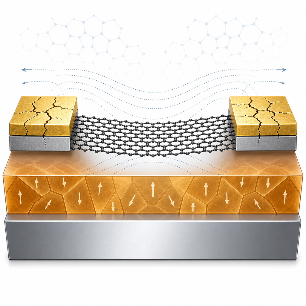
The quantitative results are striking. As-fabricated GSETs showed ambipolar behavior with electron and hole mobilities of 128 and 375 cm^2 V^-1 s^-1 and ON/OFF ratios of only ~3.5 and ~3.8. After a "forming" process of repeated strain cycling (typically by the third cycle), reversible nanocracks in the Ni/Au contacts produced antiambipolar OFF-ON-OFF behavior and an ON/OFF current ratio exceeding 10^7 at a drain bias of just 100 mV. The switching was ultra-steep, with subthreshold swings of 1.0 mV/decade (electron branch) and 1.2 mV/decade (hole branch) averaged over six orders of magnitude of current change—far below the 60 mV/decade Boltzmann tyranny that limits conventional MOSFETs. Statistical evaluation across 50 devices gave mean ON/OFF ratios of 3.6 × 10^6 (electron) and 2.9 × 10^6 (hole), with mean transconductance of 90 and 96 µS/µm respectively, values on par with state-of-the-art amplifiers. Switching threshold voltages averaged 33.9 V (VST,N) and -39.7 V (VST,P), with device-to-device variation tied to the random PZT domain distribution. Endurance measurements confirmed reproducible crack opening and closing over many strain cycles.
The technology enables steep-slope, high-ON/OFF graphene logic and switching devices without the patterning challenges of nanoribbons or the liquid-gate instability of electrochemical GFETs. Potential application areas include energy-efficient logic, RF electronics, straintronic switches, hardware security primitives, neuromorphic synapses, and flexible/stretchable smart sensors that combine sensing, storage, and compute. The authors note that the relatively high operating voltage and hysteresis window can be reduced by using thinner PZT back-gate films, which would also aid device miniaturization—pointing to concrete follow-up engineering directions. The simplicity of the GSET fabrication relative to vertical heterostructures makes it attractive for scalable manufacturing.
For researchers pursuing similar straintronic, transistor, or 2D-electronics work, the quality and transferability of the starting graphene are decisive: the device performance depends on a clean, large-area monolayer that survives wet transfer onto a sensitive piezoelectric substrate. The CVD graphene on copper foil used here is available from ACS Material's CVD Graphene line, making it a practical option for groups replicating or extending this graphene strain-effect transistor architecture.How ACS Material products were used
- CVD Graphene on Copper Foil (CVD Graphene) — “CVD-grown graphene on a Cu foil was purchased from ACS material (GFCU0101) and spin-coated with poly(methyl methacrylate) (PMMA).”
Product Performance in this StudyThe ACS Material CVD monolayer graphene on copper served as the channel material of the strain-effect transistor. After wet transfer to the PZT substrate, it provided a high-mobility ambipolar channel that retained high ON-state current and transconductance while enabling colossal ON/OFF ratios.
Related product categories
Frequently asked questionsHow does a graphene strain-effect transistor achieve a high ON/OFF current ratio?
The graphene strain-effect transistor uses a piezoelectric PZT gate to apply strain that forms reversible nanocracks in high-tensile-strength Ni/Au source/drain contacts. These nanocracks interrupt and restore current flow, producing an ON/OFF current ratio above 10^7 at 100 mV drain bias while keeping graphene's high carrier mobility intact, unlike conventional graphene field-effect transistors limited to ratios of 2-10.
What grade of CVD graphene was used to build the transistor channel?
The researchers used commercially available CVD-grown large-area monolayer graphene on copper foil, purchased from ACS Material (catalog GFCU0101). Raman spectroscopy with a 532 nm laser confirmed its monolayer character through the G band near 1600 cm^-1 and the 2D band near 2700 cm^-1. The film was wet-transferred onto the PZT substrate using a PMMA support layer.
Why is subthreshold swing important for graphene transistor performance?
Subthreshold swing measures how sharply a transistor switches between OFF and ON states. Conventional MOSFETs are limited to 60 mV/decade by the Boltzmann tyranny. The graphene strain-effect transistor achieved 1.0 mV/decade for electrons and 1.2 mV/decade for holes over six orders of magnitude of current change, enabling steep, energy-efficient switching without sacrificing drive current.