-
CVD Graphene Substrates for Epitaxial ZnO Films - Beijing University of Technology, 2014
Jun 23, 2026 | ACS MATERIAL LLCZeng, Y., Zhao, Y., & Jiang, Y. (2014). Investigate the interface structure and growth mechanism of high quality ZnO films grown on multilayer graphene layers. *Applied Surface Science*. https://doi.org/10.1016/j.apsusc.2014.02.088
Applied Surface Science · 2014
Researchers at Beijing University of Technology used ACS Material CVD multilayer graphene to grow c-axis oriented wurtzite ZnO films by PLD, confirmed by XRD, Raman and DFT.
About this research
Researchers at Beijing University of Technology used multilayer CVD graphene purchased from ACS Material to grow high-quality wurtzite ZnO films directly on graphene by pulsed laser deposition (PLD), achieving strong c-axis orientation and sharp ultraviolet near-band-edge photoluminescence at 3.323 eV. The paper, published in Applied Surface Science (2014) by Zeng, Zhao and Jiang at the Institute of Laser Engineering, combines XRD, Raman, AFM and temperature-dependent photoluminescence with density functional theory (DFT) simulations to clarify both the structural quality of the films and the chemical nature of the ZnO/graphene interface. The work establishes graphene as a viable growth template for oxide semiconductor films aimed at flexible optoelectronic devices.
Growing crystalline oxides such as ZnO directly on graphene is attractive because graphene is mechanically robust, optically transparent, electrically conductive and flexible, while ZnO is a wide-bandgap semiconductor used in solar cells, gas sensors, transparent electrodes and acoustoelectric devices. The challenge is that pristine graphene is hydrophobic and chemically inert, which usually requires seed layers or surface functionalization before oxide nucleation. Prior reports demonstrated ZnO nanorods, nanowalls and nanowires on graphene via hydrothermal or MOCVD routes, but the photoluminescence, structural quality and interface chemistry of continuous epitaxial ZnO films grown directly on graphene had not been systematically addressed. Clarifying the bonding configuration is critical for designing reproducible flexible heterostructures based on graphene and functional oxides.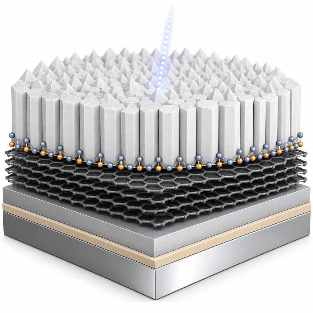
The authors purchased multilayer graphene from ACS Material, supplied on a 300 nm nickel film deposited by CVD onto a 500 nm SiO2/Si wafer. Raman spectra of the as-received material showed the characteristic D, G and 2D peaks at 1348, 1581 and 2708 cm⁻¹, with a 2D position consistent with few-layer graphene. Before deposition, the substrates were sequentially cleaned in acetone, ethanol and deionized water by ultrasonication for 5 minutes. ZnO films roughly 300 nm thick were then grown by PLD using a 248 nm KrF excimer laser (pulse width 23 ns) at fluences near 2500 mJ cm⁻² and a repetition rate of 3 Hz, under 40 Pa oxygen, at substrate temperatures of 400 °C and 600 °C and pulse counts between 10,000 and 20,000. No seed layer or surface activation step was applied to the graphene, making the ACS Material substrate the sole nucleation surface for the oxide.
XRD of the resulting ZnO films showed a dominant (002) peak at 34.5° and a (004) peak at 72.7°, with a (002) FWHM of 0.2°, demonstrating well-oriented c-axis growth perpendicular to the graphene plane. Raman spectra resolved the wurtzite E2(low) and E2(high) modes at 99 and 437 cm⁻¹ alongside the graphene D, G and 2D peaks, confirming that both phases survived the deposition. AFM revealed that increasing the pulse count from 10,000 to 20,000 at 400 °C transformed the surface from a corrugated morphology with RMS roughness of about 14 nm into a conical, island-like morphology with RMS of about 23 nm and a water contact angle of 124.5°, larger than the 108° measured on a comparable ZnO film on sapphire. Temperature-dependent photoluminescence from 80 to 150 K showed two sharp near-band-edge peaks at 3.323 and 3.312 eV with FWHM of 14 and 8 meV. At room temperature, the I_NBE/I_DL ratio reached 6.257 on graphene versus 3.169 on sapphire, and the NBE FWHM was 84 meV on graphene compared with 94 meV on sapphire, indicating superior optical quality on the ACS Material graphene substrate. DFT with ultrasoft pseudopotentials gave adsorption binding energies of 77.262 kJ/mol for C–Zn–O and 56.989 kJ/mol for C–O–Zn, and interfacial adsorption energies of 2.5907 and 3.4017 J/m² for two candidate stacks, identifying graphene–Zn–O–Zn–O as the stable interface.
The combination of strong UV emission, low deep-level emission, robust adhesion after ultrasonic cleaning, and a chemically bonded graphene–Zn interface makes this ZnO/graphene heterostructure attractive for flexible UV emitters, transparent conducting layers, photodetectors, gas sensors and ZnO-based solar cell windows. Because the graphene resides on a Ni/SiO2/Si stack, the same approach is compatible with downstream transfer onto flexible polymer substrates for wearable optoelectronics. The clarified bonding picture also gives film-growth engineers a clear target for tuning nucleation by controlling the initial Zn-rich pulses, with broader implications for epitaxy of other metal oxides such as Ga2O3, SnO2 or In2O3 on graphene templates.
For researchers working on graphene/oxide heterostructures, this study illustrates how a commercially available CVD multilayer graphene substrate can serve as a direct template for high-quality oxide thin films without seed layers. The CVD graphene-on-nickel and graphene-on-SiO2 substrates in the ACS Material catalog cover the same material class used here. Groups developing flexible UV emitters, transparent electrodes or 2D-material/oxide hybrid devices can therefore source reproducible graphene substrates suitable for PLD, sputtering or MOCVD growth from ACS Material and build on the interface model reported in this paper.How ACS Material products were used
- CVD multilayer graphene on nickel/SiO2/Si substrate (CVD Graphene) — “Graphene samples were bought from ACS Material Company. Graphene layers were grown on thin nickel film (300 nm) deposited by CVD on silicon dioxide (500 nm)/silicon wafer.”
Product Performance in this StudyThe multilayer CVD graphene served as the growth substrate for pulsed-laser-deposited ZnO. It enabled epitaxial, c-axis oriented wurtzite ZnO films with strong UV near-band-edge emission, demonstrating that the graphene supplied by ACS Material can act directly as a template for high-quality oxide semiconductor films.
Related product categories
Frequently asked questionsWhy use CVD graphene as a substrate for ZnO thin film growth?
CVD graphene provides an atomically flat, mechanically robust and chemically stable surface that is compatible with flexible device platforms. In this study, multilayer CVD graphene enabled direct c-axis oriented wurtzite ZnO growth without any seed layer, producing sharp 3.323 eV UV emission and a high I_NBE/I_DL ratio of 6.257, outperforming the same PLD ZnO on sapphire, which makes graphene attractive for flexible UV optoelectronics.
How is the ZnO bonded to the graphene surface during pulsed laser deposition?
Density functional theory calculations show that Zn atoms bond preferentially to graphene carbon, with C–Zn–O adsorption energy of 77.262 kJ/mol versus 56.989 kJ/mol for C–O–Zn. The 3d orbital of Zn overlaps with the 2p orbital of C, forming a partially covalent Zn–C bond. The most stable interface stack is graphene–Zn–O–Zn–O, with an interfacial adsorption energy of 3.4017 J/m².
What growth parameters give the best ZnO film quality on graphene by PLD?
At 400 °C, 40 Pa oxygen and 20,000 laser pulses (248 nm, 23 ns, ~2500 mJ cm⁻², 3 Hz), the ZnO film showed conical island morphology, RMS roughness near 23 nm, a water contact angle of 124.5°, and the strongest UV emission. Increasing the temperature to 600 °C degraded the UV emission, indicating that moderate temperature combined with sufficient pulse count yields the best optical quality.