-
CVD Graphene Surface Stress on Soft PDMS - Peking University, 2016
Jul 07, 2026 | ACS MATERIAL LLCDu, F. et al. (2016). Surface stress of graphene layers supported on soft substrate. *Scientific Reports*. https://doi.org/10.1038/srep25653
Scientific Reports · 2016
Peking University researchers used ACS Material CVD graphene on copper foil to measure the surface stress of single- and multilayer graphene on soft silicone.
About this research
Researchers at Peking University used CVD graphene on copper foil purchased from ACS Material to measure, for the first time, the apparent surface stress of single-layer and multilayer graphene supported on soft silicone substrates, reporting values from 58.4 mN/m for monolayer graphene up to about 120 mN/m for three or more layers. The study, published in Scientific Reports (2016), combines droplet-induced micro-deformation imaging with the Neumann triangle concept to extract a fundamental mechanical parameter that had not previously been quantified for supported graphene films. The work also demonstrates an experimental route for measuring the surface stress of arbitrary ultrathin films placed on compliant substrates.
Surface stress is a key parameter linking atomic-scale bonding to macroscopic deformation, and it strongly influences the response of nanoscale films, layered cantilevers, and flexible sensors. Graphene, being the thinnest known material, is increasingly placed on soft polymer substrates to build flexible electrodes, solar cells, artificial actuators, and ultra-sensitive tactile sensors that can detect pressures approaching the human perception limit. In such devices the apparent surface stress of the graphene–substrate composite is a principal factor governing how the system deforms under mechanical loading, and is therefore central to device design. Despite this, no direct experimental value for the apparent surface stress of supported graphene had been reported, a gap this paper closes by carefully measuring the deformation field induced by liquid droplets resting on the graphene-covered gels.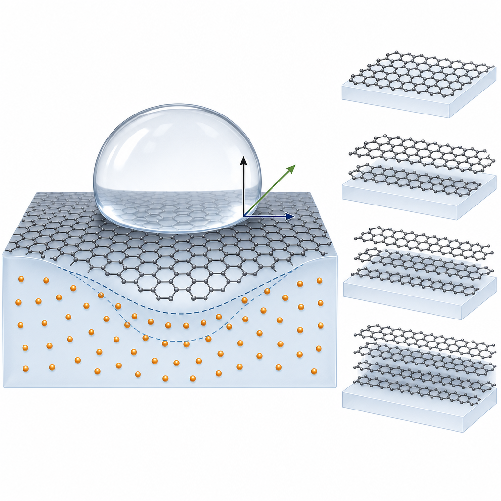
The ACS Material graphene was used as the principal experimental layer. The authors describe their samples as "chemical vapor deposition (CVD) multilayer graphene (two layers and 3~5 layers) on a copper foil (ACS Materials, USA)" together with polycrystalline single-layer graphene also purchased from ACS Material. Graphene-on-copper coupons (~2 cm) were processed by removing backside graphene with an oxygen plasma (100 W, 3 min), pressing the foil flat onto either PDMS (Sylgard 184, base:curing 75:1) or CY52-276 silicone substrates containing 200 nm fluorescent tracer beads, and then etching the copper in 0.5 M ammonium peroxydisulfate for about 30 minutes followed by repeated rinsing. Multilayer-covered substrates were prepared either by transferring as-grown multilayers in a single step or by stacking single layers on copper layer-by-layer before transfer. The soft silicone substrates were 16, 30 or 70 µm thick with Young's moduli of roughly 2–3 kPa, giving an elasto-capillary length suitable for resolving surface-stress-controlled deformation.
Glycerol and liquid paraffin droplets were placed on the graphene-covered gels and the three-dimensional displacement field of the embedded fluorescent beads was reconstructed using a spinning-disk confocal microscope (40× oil, NA 1.3). The graphene-covered substrates showed deformation profiles of the same shape as bare silicone but with significantly reduced magnitude, indicating a markedly higher resistance to the applied surface tension. The contact angle of glycerol on the graphene-covered surfaces was close to 90° (about 98°), which validates the use of the Style et al. model and the Neumann triangle to extract surface stress directly. The apparent surface stress of one layer of graphene on PDMS was measured at 58.4 ± 1.1 mN/m with glycerol and 60.6 ± 3.1 mN/m with liquid paraffin, in close agreement. Adding more layers monotonically increased the apparent surface stress, which then saturated at approximately 120 mN/m on three or more layers. This saturation directly confirms the long-standing theoretical prediction that surface stress is dominated by the topmost atomic layer plus the two layers immediately beneath it. The substrate itself was shown to contribute meaningfully to the apparent value, providing a tunable handle on graphene-system mechanics.
These results have practical implications for ultra-sensitive flexible sensors, where surface and interface stresses determine how a thin graphene film deforms in response to small lateral loads. Knowing the apparent surface stress of supported graphene films, and being able to tune it through layer number or substrate stiffness, supports the rational design of tactile sensors, strain gauges, soft electrodes, stretchable transparent conductors and artificial-skin actuators. The droplet-deformation methodology developed here is general and can be applied to other ultrathin membranes (h-BN, MoS2, polymer films) on compliant gels, opening a path to systematic mechanical characterisation of two-dimensional materials on soft substrates.
Researchers working on flexible electronics, mechanical metrology of 2D materials, or graphene-based sensor design can source the same starting material used in this study from ACS Material's CVD graphene on copper foil offering, available in single-layer, two-layer and 3–5 layer formats. The reproducible coverage, transferability, and consistent layer count that enabled the layer-dependent surface stress measurement reported here make this product class a practical choice for groups extending the work to other soft-substrate or membrane–capillarity studies.How ACS Material products were used
- CVD Graphene on Copper Foil (multilayer, 2 layers and 3-5 layers; polycrystal single-layer graphene) (CVD Graphene) — “chemical vapor deposition (CVD) multilayer graphene (two layers and 3~5 layers) on a copper foil (ACS Materials, USA)... the single layer graphene will refer to the polycrystal single layer graphene that was purchased from ACS Materials (USA)”
Product Performance in this StudyThe CVD graphene on copper foil from ACS Material served as the principal experimental specimen. After transfer onto soft silicone substrates, the graphene films supported substantial droplet-induced stresses and allowed the authors to extract apparent surface stress values, demonstrating reliable, continuous coverage from 1 to 3–5 layers.
Related product categories
Frequently asked questionsWhat is the surface stress of single-layer graphene on a soft PDMS substrate?
Based on droplet-induced deformation measurements on 16–70 μm thick PDMS (Young's modulus ~2 kPa), the apparent surface stress of one layer of CVD graphene on PDMS is 58.4 ± 1.1 mN/m measured with glycerol and 60.6 ± 3.1 mN/m measured with liquid paraffin. These values are substantially higher than the surface stress of the bare silicone substrate, showing that even a single graphene layer markedly stiffens the surface response.
How does the surface stress of supported graphene depend on the number of layers?
The apparent surface stress of graphene-covered silicone increases monotonically with layer number and saturates at approximately 120 mN/m once three or more layers are present. This saturation directly confirms the long-standing theoretical result that the surface stress is dominated by contributions from the outermost atomic layer plus the two layers immediately beneath it, with deeper layers contributing negligibly.
Why is CVD graphene on copper foil used for soft-substrate surface stress experiments?
CVD graphene on copper foil provides large-area, continuous films with reproducible layer count, which is essential for systematic layer-dependent mechanical measurements. The foil can be pressed onto soft silicone substrates and then etched away with ammonium peroxydisulfate, leaving the graphene cleanly transferred onto the gel. This procedure preserves film continuity, allowing the droplet-induced deformation to faithfully reflect the surface stress of the graphene–substrate system.