-
CVD Graphene/Si Photodetectors with Pt NPs - Zhejiang University, 2018
Jun 16, 2026 | ACS MATERIAL LLCHu, M. et al. (2018). Performance improvement of graphene/silicon photodetectors using high work function metal nanoparticles with plasma effect. *Advanced Optical Materials*. https://doi.org/10.1002/adom.201701243
State Key Laboratory of Silicon Materials School of Materials Science and Engineering Zhejiang University Hangzhou 310027 China · Advanced Optical Materials · 2018
Zhejiang University researchers used ACS Material CVD graphene on copper foil to build Gr/Si photodetectors with 1.68 × 10^7 A/W responsivity and 180 ns response.
About this research
Researchers at the State Key Laboratory of Silicon Materials, School of Materials Science and Engineering, Zhejiang University used CVD monolayer graphene on copper foil purchased from ACS Material to build graphene/silicon (Gr/Si) photodetectors whose visible-light responsivity reached 1.68 × 10^7 A/W after decoration with platinum nanoparticles. The work, published in Advanced Optical Materials (2018), demonstrates that combining a clean CVD graphene transfer with drop-cast colloidal Pt nanoparticles produces a photoconductor that is both ultrahigh in responsivity and fast (~180 ns response time), bypassing the lithographic lift-off processes typically required to fabricate plasmonic noble-metal arrays on graphene.
Graphene/silicon Schottky photodetectors are attractive because they are easy to fabricate and pair the high carrier mobility of graphene with the strong built-in field of silicon. However, the optical absorption of monolayer graphene is only about 2.3%, and pristine Gr/Si devices typically reach responsivities of only hundreds of mA/W. Plasmonic metal nanoparticles can dramatically boost absorption through localized surface plasmon resonance (LSPR), while a high-work-function metal such as platinum simultaneously dopes graphene p-type, lowering its Fermi level and strengthening the Schottky barrier. Combining both effects in a scalable, low-cost device architecture is an open challenge for next-generation visible and near-infrared photodetectors used in imaging, optical communication, and sensing.
The ACS Material CVD graphene was supplied as a single-layer (SLG) film grown on copper foil. The authors spin-coated PMMA (950 K) onto the graphene, etched the copper in ammonium persulfate, rinsed and transferred the floating film onto pre-cleaned N-type ⟨100⟩ silicon (0.05–0.1 Ω·cm) from which the native oxide had been stripped with HF. The Gr/Si stack was annealed at 520 °C in argon for 2 hours to remove residual PMMA and improve contact at the graphene–silicon interface. Ti/Au (5 nm/50 nm) contact electrodes were deposited by thermal evaporation. Finally, colloidal Pt nanoparticles, synthesized via a borohydride reduction of H2PtCl6 in the presence of oleic acid and Pluronic F127, were drop-cast onto the graphene to introduce the plasmonic and work-function-tuning layer. The graphene therefore plays the dual role of transparent electrode and active charge-transport channel.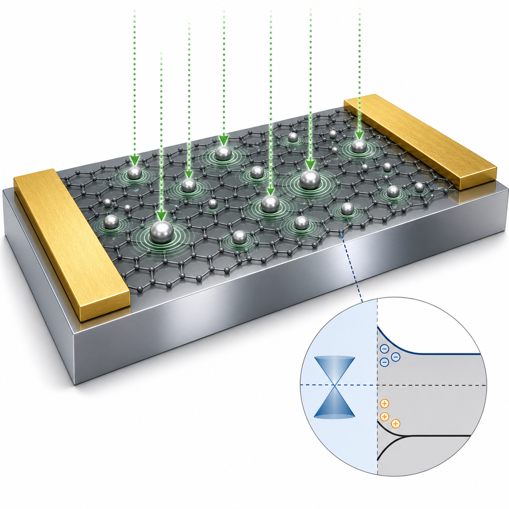
The Pt-decorated Gr/Si device delivered a visible-range responsivity of 1.68 × 10^7 A/W, more than an order of magnitude higher than an otherwise identical pristine Gr/Si reference. Kelvin probe force microscopy confirmed that Pt deposition shifted the graphene work function upward, consistent with hole doping by the high-work-function metal (Pt ~5.6 eV) and a strengthened built-in field at the Schottky junction. UV–Vis extinction spectra of the Pt NP layer showed broad plasmonic absorption in the visible range, which the authors correlate with the enhanced external quantum efficiency measured on a PVM_QEX10 system. Transient photoresponse, measured under a power-tunable 532 nm laser modulated by a Rigol signal generator and read out on a Tektronix oscilloscope, gave a rise/fall time of about 180 ns – an exceptionally fast value for graphene-based photoconductors at this wavelength and attributed by the authors to the low density of interfacial trap states created by the clean PMMA-removal anneal. The device also showed stable, reproducible switching over many on/off cycles.
The results point to several applications. The same Pt-decoration approach can be applied to Gr/Si solar cells and near-infrared detectors, to silicon-photonics-integrated graphene photodetectors for short-haul optical interconnects, and to high-speed imaging arrays where both high gain and sub-microsecond response are needed. The drop-casting route avoids costly e-beam lithography, making it compatible with wafer-scale processing. The authors suggest that further tuning of Pt nanoparticle size, shape and surface coverage – or substitution with other high-work-function plasmonic metals – could push responsivity and bandwidth even higher, and that the strategy is broadly transferable to other 2D-material/semiconductor heterojunction photoelectronic devices.
For researchers working on Gr/Si photodetectors, plasmonic 2D-material devices, or transparent-conductor optoelectronics, the quality of the starting CVD graphene is critical: the PMMA-assisted transfer and 520 °C anneal only deliver low interface-trap density if the as-grown film is uniform monolayer with minimal multilayer islands. ACS Material's CVD Graphene on Copper Foil, the product used in this study, is available to researchers building similar Schottky-junction photodetectors, plasmonic photonic devices, and graphene-transfer process development workflows.How ACS Material products were used
- CVD Graphene on Copper Foil (CVD Graphene) — “A commercial CVD grown graphene film on a copper foil (SLG, bought from ACS Material) was spin-coated with PMMA (950 K, bought from Allresist Inc.), then ammonium persulfate was utilized to etch copper and thus to release the graphene film.”
Product Performance in this StudyThe CVD monolayer graphene served as the transparent, conductive top layer of the Gr/Si Schottky photodetector. After PMMA-assisted transfer onto N-type Si, it formed a clean junction enabling responsivity up to 1.68 × 10^7 A/W and ~180 ns response time.
Related product categories
Frequently asked questionsHow do platinum nanoparticles improve graphene/silicon photodetector performance?
Platinum nanoparticles enhance Gr/Si photodetector performance through two simultaneous mechanisms. Their localized surface plasmon resonance boosts visible-light absorption in both graphene and silicon, while platinum's high work function (~5.6 eV) p-dopes the graphene, lowering its Fermi level and strengthening the built-in Schottky field. In this study, the combined effects raised responsivity to 1.68 × 10^7 A/W, an order of magnitude above pristine devices.
Why is CVD monolayer graphene on copper foil used to build Schottky-junction photodetectors?
CVD graphene on copper foil provides wafer-scale, uniform monolayer films that can be transferred to silicon to form a clean Schottky junction. Because monolayer graphene is transparent yet conductive, it functions simultaneously as a transparent top electrode and as the active channel. The PMMA-assisted transfer used here, followed by a 520 °C argon anneal, removes polymer residue and reduces interfacial trap density, enabling sub-microsecond response times.
What response time can graphene/silicon photodetectors achieve in the visible range?
In this work, a Gr/Si photoconductor decorated with platinum nanoparticles reached a response time of about 180 nanoseconds under 532 nm illumination. The authors attribute this fast response to the low density of interface trap states between the CVD graphene and silicon after PMMA removal at 520 °C, which avoids the millisecond-scale tails that often plague quantum-dot- or perovskite-sensitized graphene photodetectors.