-
CVD Graphene/Si Solar Cells with GO Coating — UC San Diego, 2016
Jun 25, 2026 | ACS MATERIAL LLCYavuz, S. et al. (2016). Graphene oxide as a p-dopant and an anti-reflection coating layer, in graphene/silicon solar cells. *Nanoscale*. https://doi.org/10.1039/c5nr09143h
Nanoscale · 2016
UC San Diego researchers used ACS Material CVD monolayer graphene to build Gr/Si solar cells with GO as p-dopant and anti-reflection coating, tripling efficiency.
About this research
At the University of California San Diego, S. Yavuz, C. Kuru, D. Choi, A. Kargar, S. Jin, and P. R. Bandaru demonstrated that CVD monolayer graphene from ACS Material, when combined with a spin-coated graphene oxide (GO) overlayer, produces graphene/silicon (Gr/Si) Schottky-junction solar cells with roughly three-fold higher power-conversion efficiency and improved environmental stability versus uncoated devices. Published in Nanoscale (2016, DOI: 10.1039/C5NR09143H), the work shows that a single GO film can simultaneously serve as a p-type dopant for graphene, as an oxidation barrier protecting the underlying silicon, and as an anti-reflection coating (ARC) when its thickness is tuned. This dual-functional, single-layer approach replaces multi-step doping/passivation/ARC stacks typical in earlier Gr/Si photovoltaic work.
Graphene/silicon heterojunction solar cells are attractive because graphene replaces conventional transparent conductors and emitter doping simultaneously, while the n-Si side handles light absorption. However, raw Gr/Si cells suffer from low efficiency, surface oxidation of the silicon at the junction, and rapid degradation of acid-based p-dopants such as HNO3 or SOCl2. Researchers have therefore pursued surface texturing, chemical doping, and dielectric ARC layers to boost performance — but these strategies are usually applied as separate processing steps and rarely address device stability. A single coating that consolidates these functions would streamline fabrication and extend operating lifetime, both of which are important for translating Gr/Si photovoltaics from lab demonstration toward practical use.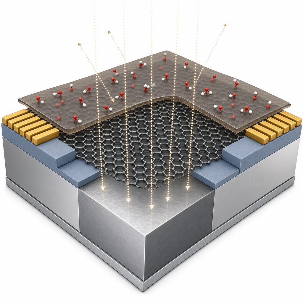
In the fabrication flow, an n-type Si wafer (0.5–1 Ω·cm) was passivated with a 350 nm PECVD SiO2 layer, after which a 3 mm × 3 mm window was opened by photolithography and a 6:1 buffered oxide etch. Au/Ti front contacts and an Al back contact provided Ohmic electrodes. The CVD monolayer graphene obtained from ACS Material was then wet-transferred onto the exposed silicon window to form the Schottky junction. Graphene oxide synthesized by a modified Hummers' method was dispersed in deionized water at 1 mg/mL and spin-coated on top of the Gr/Si stack, with SEM confirming uniform film coverage. The CVD graphene therefore serves as the active transparent electrode in direct contact with silicon, while the GO overlayer modulates its work function and the optical reflectance of the device. The authors emphasize that without high-quality monolayer graphene, the GO coating cannot deliver simultaneous doping and anti-reflection benefits, making the ACS Material CVD graphene central to the device architecture.
The combined GO coating produced approximately a three-fold enhancement in power-conversion efficiency relative to bare Gr/Si cells. The authors attribute this improvement to two cooperating mechanisms. First, GO transfers charge to the underlying graphene, raising its Fermi level offset and increasing the built-in potential at the Gr/Si Schottky junction, which boosts the open-circuit voltage. Second, the GO film, when its thickness is matched to the relevant visible wavelengths, behaves as an ARC: GO is reported to be highly transparent from the UV to the near-IR, so an appropriately thick layer reduces front-surface reflection without parasitic absorption. The authors also report enhanced device stability — performance was maintained over a 20-day ambient period, which the paper notes is among the most durable Gr/Si solar cell results reported up to that time. They credit this stability to the chemical inertness of GO in ambient air and to its role as a physical barrier that suppresses silicon oxidation at the junction interface, in contrast to volatile acid dopants whose effect typically decays over hours to days.
The results have direct implications for low-cost silicon photovoltaics, flexible solar cells using transferred graphene electrodes, and any Schottky-junction device that benefits from simultaneous doping and optical management. Because GO is solution-processable, the approach is compatible with spin coating, spray coating, and roll-to-roll deposition, opening a route to scalable, multifunctional coatings on graphene-based optoelectronics. Follow-up work pointed to by the authors includes systematic optimization of GO thickness for matched ARC behavior, exploration of reduced GO or chemically modified GO variants for stronger p-doping, and integration with textured silicon surfaces for further light-trapping gains. The dual-function strategy may also transfer to other 2D-material/semiconductor junctions such as MoS2/Si or WS2/Si cells where surface stability is similarly limiting.
For researchers replicating or extending this work, the key materials enabler is high-quality CVD monolayer graphene on copper foil suitable for wet transfer onto silicon — the same class of material supplied by ACS Material under its CVD Graphene product line. Groups working on graphene/silicon photovoltaics, Schottky-junction photodetectors, or transparent electrodes for flexible devices can source comparable wafer-scale CVD graphene from ACS Material to support similar experiments. The paper itself stands as a useful benchmark: it shows that pairing well-transferred CVD graphene with a simple solution-processed GO overlayer can simultaneously address efficiency and stability, two of the longest-running challenges in this device family.How ACS Material products were used
- CVD Graphene on Copper Foil (monolayer) (CVD Graphene) — “Chemical Vapor Deposition (CVD) based mono-layer graphene (MLG, obtained from ACS Materials) was placed on the Si substrate using a wet transfer method”
Product Performance in this StudyThe CVD monolayer graphene from ACS Material served as the transparent conductive electrode forming the Schottky junction with n-Si. Combined with a graphene oxide coating that doped the graphene and acted as an anti-reflection layer, the device achieved a three-fold efficiency enhancement and 20-day ambient stability.
Related product categories
Frequently asked questionsHow does graphene oxide improve graphene/silicon solar cell efficiency?
Graphene oxide deposited on top of CVD graphene acts in two ways. It transfers charge to graphene, p-doping it and increasing the built-in potential of the graphene/silicon Schottky junction, which raises open-circuit voltage. At an appropriate thickness, the same GO film also functions as an anti-reflection coating because it is highly transparent from the UV to the near-infrared, reducing front-surface reflection without significant parasitic absorption.
Why is CVD monolayer graphene preferred for silicon Schottky-junction solar cells?
CVD monolayer graphene combines high optical transparency with sufficient lateral conductivity to serve as both the transparent electrode and the doped emitter of a silicon Schottky-junction solar cell. Its uniform single-layer character, achievable through wet transfer onto patterned silicon windows, ensures a well-defined junction interface. ACS Material supplies CVD graphene on copper foil designed for exactly this kind of transfer onto device substrates.
How stable are graphene/silicon solar cells with graphene oxide coatings?
The Nanoscale 2016 study reports that GO-coated Gr/Si solar cells retained their performance over a 20-day ambient air period, which the authors note is among the most durable Gr/Si solar cells reported at that time. Stability comes from GO's chemical inertness in air and its barrier role suppressing silicon oxidation at the junction, in contrast to acid dopants such as HNO3 whose effect typically decays quickly.