-
CVD Monolayer Graphene Si Nanopillar Photodetector - Fudan University, 2021
Jun 12, 2026 | ACS MATERIAL LLCFeng, B. et al. (2021). A broadband photoelectronic detector in a silicon nanopillar array with high detectivity enhanced by a monolayer graphene. *Nano Letters*. https://doi.org/10.1021/acs.nanolett.1c01244
Fudan University · Nano Letters · 2021
Fudan University integrated ACS Material CVD monolayer graphene on Si nanopillars, achieving 1.43 × 10^13 Jones detectivity over 450–1100 nm at room temperature.
About this research
Fudan University researchers developed a broadband silicon nanopillar photoelectronic detector enhanced by transferring ACS Material CVD monolayer graphene onto the pillar array, achieving a specific detectivity of 1.43 × 10^13 Jones across 450–1100 nm at room temperature. By forming a graphene/Si Schottky contact on top of a buried p–n junction, the team simultaneously reduced dark current and boosted photocurrent, reaching photovoltage responsivity exceeding 10^6 V/W and an external quantum efficiency of 74.8% at 860 nm. The architecture is compatible with CMOS read-out integration, pointing toward focal plane array chips for visible to near-infrared imaging.
Why this research matters: Photodetectors are central to environmental surveillance, optical communications, machine vision, and AI-driven imaging, but commercial silicon avalanche diodes typically require high reverse bias (around 12 V), limiting further miniaturization. Zero-bias photovoltaic detectors based on Si nanowire or nanopillar arrays have been explored for their strong light trapping and reduced dark current, yet their detectivity and responsivity have remained below the bar set by bulk Si or III–V devices. Hybridizing silicon nanostructures with two-dimensional materials offers a promising route, because graphene contributes broadband absorption, high carrier mobility, and a tunable Schottky barrier with Si. Demonstrating a graphene/Si nanopillar/p–n junction stack that combines all of these benefits in a single, CMOS-friendly platform addresses an open gap in low-bias, broadband, room-temperature photodetection.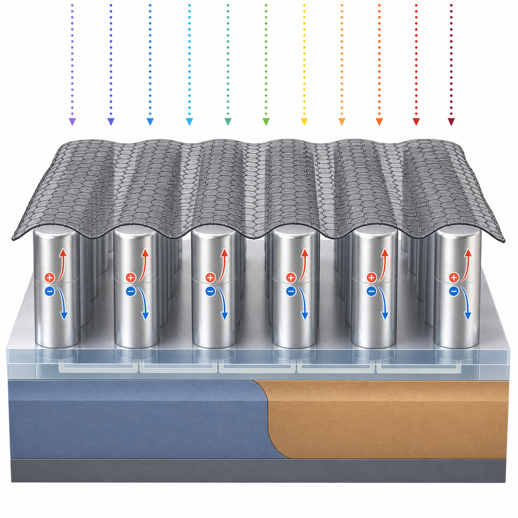
How the ACS Material product was used: The detector was fabricated on a 500 µm Si wafer with a 3 µm-thick n-type layer over a p-type substrate (boron and phosphorus doping ~10^16 cm^-3). Vertical Si nanopillars with diameters of 0.5, 1, and 3 µm and height 2.75 µm were defined by e-beam lithography and inductively coupled plasma etching in SF6/C4F8 chemistry. Hydrogen silsesquioxane was spin-coated between pillars, and a 13 nm ITO layer was sputter-deposited as a transparent interconnect. After removing the aluminum mask and native oxide with HCl and HF, monolayer CVD graphene from ACS Material was transferred onto the n-type Si nanopillar tops to form the Schottky junction and act as the top electrode. AFM measured the transferred film at about 0.37 nm thick, confirming a single layer. The graphene therefore plays a dual role as broadband absorber and as one half of the rectifying graphene/n-Si interface.
Key results: Compared with the otherwise identical nanopillar detector without graphene, the graphene-covered device showed dramatically improved electrical and optical metrics. Dark current dropped from ~21 nA to ~0.97 nA at –0.4 V, yielding clean rectifying behavior with a fitted Schottky barrier height of 0.683 eV and an ideality factor of 1.6. Under 860 nm illumination at 500 µW/cm^2, the device produced a photocurrent on the order of 10^-6 A at zero bias with an open-circuit voltage of 0.245 V, corresponding to a photosensitivity of 6.4 × 10^4. The photocurrent responsivity peaked at ~0.52 A/W, equivalent to 74.8% external quantum efficiency at 860 nm. Photovoltage responsivity exceeded ~10^6 V/W under a low light intensity of 100 nW/cm^2, making the device suitable for weak-signal detection. The specific detectivity reached 1.43 × 10^13 Jones at 860 nm and remained high across 450–1100 nm. TCAD simulations attributed the enhancement to three mechanisms: internal photoemission of hot carriers across the graphene/Si Schottky barrier, carrier separation within the depletion region near graphene/n-Si, and additional photocurrent and photogating from the underlying p–n junction. The reported detectivity is competitive with commercial InGaAs and Ge photodetectors at the same wavelengths.
Applications and outlook: The device targets broadband imaging from the visible into the near-infrared, including silicon-compatible 850–860 nm data communication links used with vertical-cavity surface-emitting lasers (VCSELs). Because both the silicon nanopillar etch and the graphene transfer are compatible with standard CMOS back-end processing, the platform is well positioned for monolithic integration into focal plane array image sensors, low-light surveillance cameras, LiDAR receivers, and on-chip optical interconnects. The reduced dark current and zero-bias operation are particularly attractive for low-power and portable systems. Future work suggested by the paper includes scaling the array, refining the Schottky interface, and exploring operation at higher temperatures while preserving the high detectivity and broadband response demonstrated here.
Why this matters for researchers: For groups working on graphene/silicon Schottky photodetectors, hybrid 2D–3D optoelectronics, and CMOS-compatible imaging arrays, the quality of the transferred graphene critically determines barrier uniformity and dark current. ACS Material's CVD monolayer graphene served effectively as both the absorber and the Schottky electrode in this study, with the resulting detectors approaching III–V performance levels. Researchers pursuing similar device architectures can source comparable CVD graphene on copper foil and graphene-on-substrate options from ACS Material's CVD graphene catalog to reproduce or extend this work.How ACS Material products were used
- CVD Monolayer Graphene (transferred onto Si nanopillars) (CVD Graphene) — “Monolayer CVD-grown graphene (ACS MATERIAL, LLC) was finally transferred onto the top of the Si nanopillars to form Schottky contacts, which also served as a top electrode.”
Product Performance in this StudyThe ACS Material monolayer CVD graphene acted as the Schottky junction partner and transparent top electrode. Its integration reduced dark current from ~21 nA to ~0.97 nA at -0.4 V and raised specific detectivity to 1.43 × 10^13 Jones with quantum efficiency of 74.8% at 860 nm.
Related product categories
Frequently asked questionsHow does monolayer graphene improve the detectivity of a silicon nanopillar photodetector?
Monolayer graphene transferred onto Si nanopillars forms a Schottky junction that reduces dark current from about 21 nA to 0.97 nA at -0.4 V while contributing extra photocurrent through hot-carrier internal photoemission. Combined with the underlying p–n junction, this raised the specific detectivity to 1.43 × 10^13 Jones at 860 nm, more than an order of magnitude better than the equivalent device without graphene.
What wavelengths can a graphene/silicon nanopillar photodetector cover?
The graphene/Si nanopillar/p–n junction photodetector demonstrated broadband response from 450 nm to 1100 nm at room temperature, spanning the entire visible range and reaching well into the near-infrared. This range matches silicon's absorption window and is suitable for VCSEL-based optical communication at 850–860 nm as well as broadband imaging applications.
Why is CVD monolayer graphene preferred over multilayer graphene for Schottky photodetectors?
Monolayer CVD graphene offers high optical transparency, large carrier mobility, and a well-defined Schottky barrier with silicon, allowing it to act simultaneously as light absorber and transparent top electrode. AFM confirmed the transferred film was about 0.37 nm thick. Thicker graphene would increase parasitic absorption above the junction and reduce the photocurrent reaching the silicon, lowering quantum efficiency.