-
CVD Multilayer Graphene for Thermoelectrics - Universitas Gadjah Mada, 2024
Jul 10, 2026 | ACS MATERIAL LLCRositawati, D. N. et al. (2024). Enhancing thermoelectric properties of multilayer graphene with Au deposition. *Materials Chemistry and Physics*. https://doi.org/10.1016/j.matchemphys.2024.129295
Materials Chemistry and Physics · 2024
Universitas Gadjah Mada uses ACS Material CVD multilayer graphene on Cu foil and Au deposition to boost Seebeck coefficient 7× and power factor 24×.
About this research
Researchers at Universitas Gadjah Mada used multilayer CVD graphene on copper foil purchased from ACS Material to investigate how thin gold deposition modifies the thermoelectric response of graphene, reporting a Seebeck coefficient rising from 0.66 μV/K for pristine graphene to 4.67 μV/K at 528 K and a 24-fold enhancement in power factor. The study combines Raman spectroscopy, SEM-EDX mapping, and four-probe thermoelectric measurements with first-principles DFT and Boltzmann transport calculations to explain how Au adatoms tune carrier concentration and introduce structural disorder that improves thermopower while keeping electrical resistivity nearly constant. The work provides a clear experimental and theoretical picture of metal-adatom doping on commercially available CVD graphene.
Thermoelectric materials convert waste heat into electricity and are increasingly important for automotive, aerospace, and microelectronic applications. Graphene is attractive because of its high carrier mobility, mechanical flexibility, and chemical stability, but its very high thermal conductivity (~5000 W/m·K) and absence of a bandgap suppress the Seebeck coefficient and the dimensionless figure of merit ZT. Strategies to overcome these limitations include defect engineering, heteroatom doping, nanostructuring, and adsorption of metal adatoms that locally modify the band structure. Gold is particularly interesting because it resists oxidation, forms an ohmic interface with graphene through physisorption, and—because its work function (5.47 eV) exceeds that of graphene (~4.5 eV)—drives electron transfer from graphene to Au, producing p-type doping. Prior to this work, no experimental study had systematically examined Au-deposited multilayer graphene for thermoelectric use.
The ACS Material CVD multilayer graphene was supplied on single-sided copper foil with 35 μm thickness in a 2 in × 2 in format. The authors cut the as-received material into 2 cm × 0.5 cm strips and deposited Au directly onto the graphene surface using a LUXOR Au sputter coater at thicknesses of 7 nm (MLG-Au1) and 10 nm (MLG-Au2), with an unmodified strip serving as MLG-Pristine reference. Raman spectroscopy at 532 nm excitation tracked the D, G, and 2D bands; SEM-EDX (JEOL JSM-6510LA) mapped Au, C, and Cu distribution; and an LSR-4 Linseis system measured Seebeck coefficient and resistivity from 332 K to 552 K under a low-pressure helium atmosphere using a four-point probe at 100 mA. The Cu foil remained as the supporting substrate during thermoelectric measurement, contributing measurable background to the absolute Seebeck values reported. This direct use of the as-grown graphene/Cu stack made the workflow straightforward and reproducible.
Raman analysis confirmed Au-induced doping and defect generation. The G peak shifted from 1576 cm⁻¹ (pristine) to 1572 cm⁻¹ (MLG-Au1) and 1580 cm⁻¹ (MLG-Au2), while the ID/IG ratio rose markedly from 0.19 to 0.56 in MLG-Au2, indicating a higher density of structural defects. The I2D/IG ratio decreased from 0.37 to 0.25, consistent with multilayer character and Au-induced disorder. SEM-EDX mapping showed Au coverage of 2.19 at% on MLG-Au1 and 3.98 at% on MLG-Au2, with the gold particles up to 1 μm in diameter and more densely distributed in the thicker deposit. Thermoelectric measurements showed all samples behaving as p-type conductors with positive Seebeck coefficients that rose with temperature. The Seebeck coefficient reached 3.17 μV/K for MLG-Au1 and 4.67 μV/K for MLG-Au2 at 528 K, compared with 0.66 μV/K for pristine graphene. Power factors increased from 0.014 mW/m·K² (pristine) to 0.35 mW/m·K² (MLG-Au1) and 0.77 mW/m·K² (MLG-Au2), an 11-fold and 24-fold improvement, respectively. Average resistivity remained nearly unchanged (~23 × 10⁻⁹ Ω·m), confirming that the improvement comes from defect-driven enhancement of thermopower rather than from conductivity loss. DFT calculations on 6.25% Au-doped graphene corroborated the experimental trend, predicting a Seebeck coefficient increase from 464 to 474 μV/K at 300 K and a Fermi-level shift of ~0.41 eV consistent with p-type charge transfer to Au.
The findings demonstrate that gold deposition is a simple, scalable route to tune the thermoelectric response of CVD-grown multilayer graphene without sacrificing electrical conductivity. Such defect-engineered graphene films could contribute to flexible thermoelectric generators for low-grade waste-heat recovery in wearable electronics, automotive sensors, and aerospace systems where weight and mechanical compliance matter. The combination of Raman fingerprinting and four-probe transport measurement also provides a workflow that other groups can adopt to screen graphene/metal interfaces for energy applications. Future work suggested by the authors includes deliberately introducing additional structural imperfections, exploring alternative metal adatoms, and decoupling the contribution of the Cu substrate to obtain intrinsic graphene thermopower values.
For researchers pursuing similar thermoelectric, sensor, or flexible-electronics studies, this paper underscores the utility of starting from a well-characterized CVD graphene/Cu source. The ACS Material CVD Graphene on Copper Foil used here is available in research-scale formats and provided the consistent multilayer baseline required to resolve subtle Au-induced shifts in Raman and Seebeck signals. Reliable starting substrates remain critical to attributing performance changes to deliberate processing steps rather than to film-to-film variability.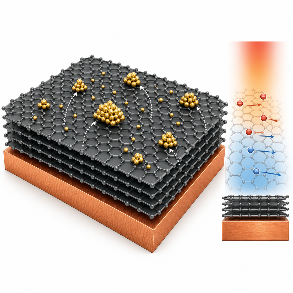
How ACS Material products were used
- CVD Graphene on Copper Foil (multilayer, 2 in × 2 in, Cu thickness 35 μm) (CVD Graphene) — “Multilayer CVD graphene (2 in × 2 in) on single-sided copper (Cu) foil with a thickness of 35 μm was purchased from the ACS Materials, LLC (www.acsmaterial.com).”
Product Performance in this Study
The multilayer CVD graphene on copper foil served as the base substrate for Au deposition and all thermoelectric measurements. Its uniform quality enabled clear Raman and SEM-EDX characterization and provided a reliable baseline against which Au-deposition–induced thermoelectric enhancement (Seebeck coefficient rising from 0.66 to 4.67 μV/K and a 24-fold power factor increase) was demonstrated.
Related product categories
Frequently asked questions
How does Au deposition improve the thermoelectric properties of multilayer graphene?
Gold atoms sputter-deposited onto multilayer CVD graphene introduce structural defects and act as a p-type dopant because gold's work function (5.47 eV) exceeds graphene's (~4.5 eV), driving electron transfer from graphene to Au. The resulting defect scattering and tuned hole concentration raise the Seebeck coefficient from 0.66 μV/K to 4.67 μV/K at 528 K and increase the power factor by up to 24 times, without significantly raising electrical resistivity.
Why use multilayer CVD graphene on copper foil for thermoelectric research?
Multilayer CVD graphene on copper foil provides a uniform, large-area, high-quality starting material suitable for surface treatments such as metal deposition or plasma processing. The copper foil acts as both growth substrate and a mechanical support during measurements, while the multilayer character improves carrier transport relative to monolayer graphene. Researchers can directly characterize the as-received film with Raman, SEM-EDX, and four-probe transport without additional transfer steps.
What does the ID/IG Raman ratio tell us about Au-doped graphene?
The ID/IG ratio is a quantitative indicator of structural disorder in graphene. In this study, ID/IG rose from 0.19 in pristine graphene to 0.56 after 10 nm Au deposition, indicating a higher density of defects, grain boundaries, and amorphous regions. This increase correlates directly with the enhanced Seebeck coefficient and power factor, confirming that defect-induced phonon scattering and band modification drive the thermoelectric improvement.