-
CVD Trilayer Graphene Anode for OLEDs - NUPT, 2018
Jun 18, 2026 | ACS MATERIAL LLCZhang, Q. et al. (2018). Negative differential resistance and hysteresis in graphene-based organic light-emitting devices. *Journal of Materials Chemistry C*. https://doi.org/10.1039/c7tc05148d
Key Laboratory for Organic Electronics and Information Displays & Jiangsu Key Laboratory for Biosensors · Journal of Materials Chemistry C · 2018
Trilayer CVD graphene from ACS Material enables OLED anodes with 41.6 cd/A efficiency after current annealing eliminates PMMA-induced NDR and hysteresis.
About this research
Researchers at the Key Laboratory for Organic Electronics and Information Displays & Jiangsu Key Laboratory for Biosensors (Nanjing University of Posts & Telecommunications) used trilayer CVD graphene supplied by ACS Material to fabricate phosphorescent organic light-emitting diodes (OLEDs), and uncovered that negative differential resistance (NDR) and current-voltage hysteresis - until now overlooked in graphene OLEDs - are governed by residual poly(methyl methacrylate) (PMMA) left behind during graphene transfer. The team showed that a simple electrical pre-scan acts as a current-annealing step that decomposes the polymer film, raising luminous efficiency from 30.9 to 41.6 cd A^-1, and up to 89.2 cd A^-1 with a half-ball outcoupling lens. The work, published in Journal of Materials Chemistry C (2018), reframes graphene-anode OLED design around interfacial polymer chemistry rather than only sheet resistance and work function.
Replacing brittle indium tin oxide (ITO) with graphene is one of the clearest routes to mechanically flexible OLEDs for displays and solid-state lighting. However, graphene anodes have historically suffered low electroluminescence efficiency due to low work function and high sheet resistance, and a great deal of literature focuses on p-type chemical doping (HNO3, AuCl3, MoO3, V2O5) to mitigate this. What has been missing is a systematic look at the transfer-process artifacts that sit at the graphene/hole-injection-layer interface. PMMA-supported wet transfer is standard for CVD graphene, but trace polymer almost always remains. This paper demonstrates that the residue is not merely a contamination nuisance: it actively drives electrical bistability, NDR, and emission instability in working OLEDs - failure modes that masquerade as graphene 'quality' problems and which limit yield, brightness, and lifetime of flexible devices.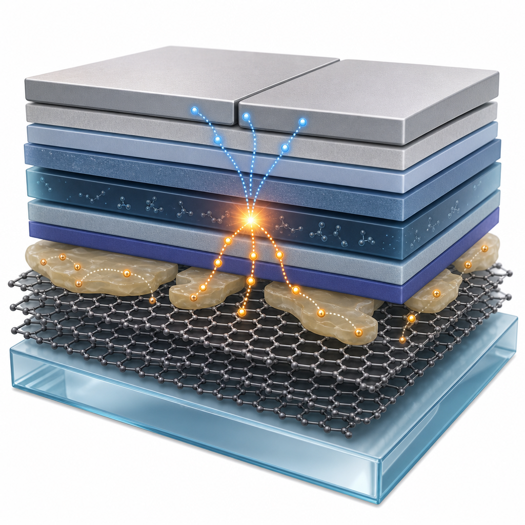
The ACS Material trilayer CVD graphene was received pre-mounted on a flexible carrier substrate. The authors lifted the graphene off in water, transferred it onto target glass, and rinsed three times with room-temperature acetone (or 60 °C acetone for a 'cleaned' control). After 6 min UV-ozone treatment, two-step PEDOT:PSS spin-coating produced a 70 nm hole injection layer; sheet resistance dropped from 470 to 160 Ω/sq while transparency went from 91% to 85% at 550 nm. Raman mapping confirmed predominantly trilayer character. The graphene served as the anode in a phosphorescent OLED using PO-01 (Iridium(III)bis(4-phenylthieno[3,2-c]pyridinato)acetylacetonate) doped into a 26DCzPPy:TAPC host, with TmPyPb electron transport, LiF/Al cathode. Critically, the authors then applied 5 repeated cyclic J-V scans (0 → 5 V → -5 V → 0) before measuring device performance - this is the current-annealing step that triggers PMMA decomposition.
Without pre-scans, the J-V curves displayed pronounced NDR with an abrupt current drop near 5 V and an on/off ratio of four orders of magnitude between conductivity states. After five cyclic scans, NDR was eliminated in 85% of devices, turn-on voltage dropped from 3.9 to 2.9 V, and luminance jumped from 23,240 to 59,548 cd m^-2 at 14 V (a 156% increase). Current efficiency rose from 30.9 to 41.6 cd A^-1, a 35% gain. With a 1.922-refractive-index half-ball outcoupling lens, the device reached 76,098 cd m^-2 and 89.2 cd A^-1, nearly matching the ITO control (52.2 cd A^-1; 89.0 cd A^-1 with lens). XPS C 1s analysis confirmed the mechanism: peaks corresponding to sp^3 C-C (285.6 eV), C-O (286.7 eV), and O-C=O (288.35 eV) of PMMA all weakened after 2 mA current pre-scanning, evidencing Joule-driven decomposition. Low-temperature (77 K) measurements ruled out resonant tunnelling and supported an oxygen-vacancy filament model in which Vo migration through the PMMA island creates and ruptures conductive paths under bias. Trapped-charge-limited-current fits further showed that bulk organic traps contribute the remaining non-NDR hysteresis, which the cyclic scan also fills.
The implications extend well beyond OLED brightness numbers. Because the technique replaces high-temperature sintering with an electrical pre-scan, it is directly compatible with flexible plastic substrates that would warp or yellow above ~150 °C - a critical enabler for foldable displays, wearable lighting, and roll-to-roll graphene electronics. The same residue-driven NDR mechanism likely affects graphene-based perovskite and organic solar cells, photodetectors, and field-effect transistors, where PMMA-transferred graphene is ubiquitous. The authors note that current annealing can be applied either to finished devices or to bare graphene sheets, suggesting straightforward integration into manufacturing flows.
For researchers developing transparent flexible electrodes, this study underscores the value of starting with consistent, well-characterized CVD graphene. ACS Material supplies CVD graphene on multiple substrates - copper foil, SiO2, quartz, PET, and Trivial Transfer® formats - that map directly onto the trilayer transferred film used here. Groups working on graphene-based OLEDs, photovoltaics, or biosensors can pair these starting materials with the current-annealing protocol described in this paper to reduce interfacial trap density and improve device reproducibility on flexible substrates.How ACS Material products were used
- Trivial Transfer® Graphene (trilayer CVD graphene) (Trivial Transfer Series) — “Graphene in this work was bought from ACS Material, which was synthesized with chemical vapor deposition method and transferred onto flexible substrates to form a trilayered structure.”
Product Performance in this StudyThe trilayer CVD graphene served as the transparent anode of the OLEDs. After current-annealing to remove PMMA residue inherent to the transfer process, the graphene electrode supported orange-yellow phosphorescent OLEDs with luminous efficiency rivalling ITO controls (41.6 cd A^-1, 89.2 cd A^-1 with half-ball lens).
Related product categories
Frequently asked questionsWhat causes negative differential resistance in graphene-based OLEDs?
Negative differential resistance (NDR) in graphene-based OLEDs originates from poly(methyl methacrylate) (PMMA) residue left on the graphene surface after wet transfer. Under bias, oxygen vacancies migrate through the PMMA island to form a conductive filament; at higher bias, the filament ruptures as the polymer is depleted of oxygen vacancies, producing the abrupt current drop characteristic of NDR. Bulk organic traps further contribute to hysteresis.
How does current annealing improve graphene OLED performance?
Current annealing applies repeated cyclic voltage scans (e.g., five sweeps from 0 to +5 V to -5 V to 0) before measuring OLED emission. The resulting Joule heating decomposes residual PMMA on the graphene anode, eliminating NDR in about 85% of devices. In this work it raised luminance from 23,240 to 59,548 cd m^-2 and current efficiency from 30.9 to 41.6 cd A^-1, reaching 89.2 cd A^-1 with a half-ball lens.
Why is CVD graphene a good replacement for ITO in flexible OLEDs?
CVD graphene combines high optical transparency (around 85-91% in the visible), reasonable sheet resistance after doping, and outstanding mechanical flexibility that ITO cannot match because indium tin oxide is brittle and cracks under bending. Trilayer CVD graphene transferred onto plastic or glass substrates can serve as a transparent anode in OLEDs and other optoelectronics, enabling foldable displays and wearable lighting if interfacial residues are properly managed.