-
Graphene as a Solid-State Diffusion Barrier - University of Florida, 2014
May 26, 2026 | ACS MATERIAL LLCMorrow, W. K., Gila, B. P., & Pearton, S. J. (2014). (Invited) The Use of Graphene as a Solid State Diffusion Barrier. *ECS Transactions*. https://doi.org/10.1149/06104.0371ecst
ECS Transactions · 2014
University of Florida researchers used ACS Material CVD graphene on Si and SiO2 to block Ti silicide formation up to 900 °C and prevent Cu diffusion at 825 °C.
About this research
Researchers at the University of Florida used CVD graphene on Si and SiO2 substrates supplied by ACS Material to demonstrate that single- and double-layer graphene can serve as an effective solid-state diffusion barrier, inhibiting titanium silicide formation up to 900 °C and preventing copper diffusion into SiO2 after anneals as high as 825 °C. The work, published in ECS Transactions in 2014 by W. K. Morrow, B. P. Gila, and S. J. Pearton of the Department of Materials Science and Engineering at the University of Florida, distinguishes the failure modes of graphene barriers when paired with chemisorbed (Ti) versus physisorbed (Cu) metals. The conclusions support graphene as a candidate ultrathin barrier for back-end semiconductor metallization.
Diffusion barriers between metallization layers and underlying Si or dielectric layers are a long-standing requirement in CMOS interconnect technology. As copper interconnect dimensions shrink, the International Technology Roadmap for Semiconductors has called for robust ultrathin diffusion barriers to manage RC delay. Traditional barriers such as Ta, TaN, TiN, WN, and Ru must be thick enough to be continuous yet thin enough to leave room for the conductor, a conflict that worsens at each node. Graphene's atomic thinness, mechanical strength (Young's modulus ~1 TPa), high thermal conductivity (~5,000 W/m·K), and chemical stability make it an attractive barrier candidate. However, because graphene has only two surfaces and no bulk, whether it can actually block metal diffusion depends on the interfacial chemistry with the specific metal in contact, which had not been systematically tested in solid-state metallization stacks before this work.
The team obtained 10 mm square single-layer (SLG) and double-layer (DLG) graphene samples on either 300 nm thermal SiO2 or (100) Si from ACS Material. The graphene covered roughly an 8 mm square central region, leaving uncoated peripheral areas that served as built-in controls on every sample. Raman spectroscopy at 514 nm verified the G band near 1580 cm⁻¹ and 2D band near 2700 cm⁻¹ with low D-band intensity, confirming single- and double-layer character. Titanium (100 nm) and copper (100 nm) films were then e-beam deposited (base pressure 10⁻⁷ Torr) on top, and the stacks were rapid-thermal annealed in N2 in 100 °C increments from 200 to 900 °C for 10 minutes per step using an SSI Solaris 150 RTP. Four-point probe sheet resistance, profilometry after selective Ti etch in 5:1:1 H2O:H2O2:NH4OH, cross-sectional STEM, and XPS were used to track silicide formation, residual Ti thickness, and Cu penetration.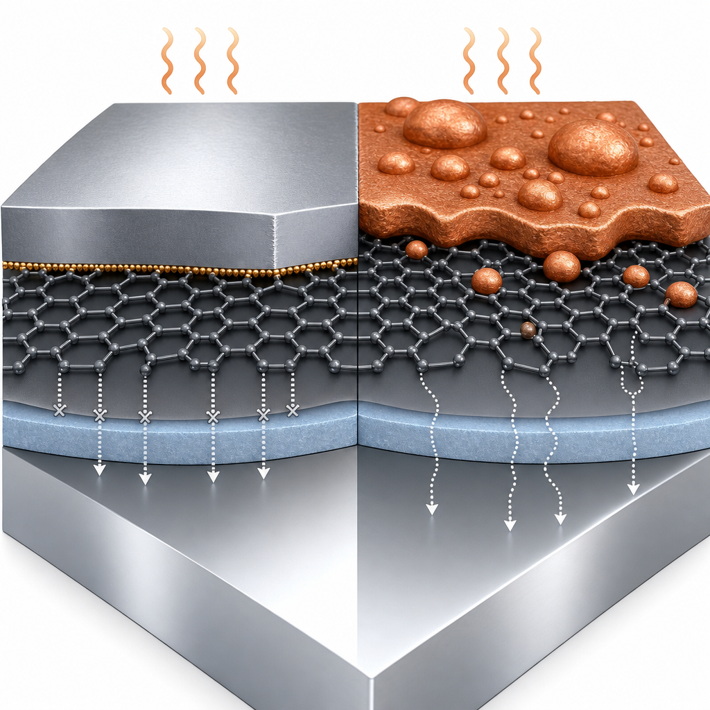
For Ti/Si controls, sheet resistance rose to ~16 Ω/sq at 400 °C (C49 TiSi2) and dropped to ~0.8 Ω/sq above 650 °C as the C54 TiSi2 phase formed, fully consuming the 100 nm Ti layer at 600 °C. In stark contrast, Ti/SLG/Si and Ti/DLG/Si samples retained the full 100 nm of unreacted Ti at 600 °C, with sheet resistance of 16-19 Ω/sq. SLG broke down at 700 °C, but DLG continued to suppress silicidation: at 800 °C only ~60% of the Ti had reacted, and DLG sheet resistance never matched the silicided control even at 900 °C. Cross-sectional TEM confirmed a sharp Ti/DLG/Si interface at 600 °C versus complete silicidation in the unprotected control. The authors attribute the barrier action to a thin TiC layer formed spontaneously at the Ti/graphene interface during deposition, which blocks Si out-diffusion to the Ti front. For Cu, copper agglomerated on the graphene surface at 600 °C and delaminated by 825 °C because of weak physisorption and low C solubility in Cu, but XPS on etched samples showed no Cu in the SiO2 underneath any graphene-protected region, while Cu/SiO2 controls showed clear Cu Cu2p3 signal. Raman after 825 °C anneals confirmed the graphene was still intact, though more defective.
These findings indicate two distinct barrier regimes. Chemisorbing metals (Ti, and by analogy Ni, Co, Ru, Pd) can form carbide-based interlayers that turn graphene into a sacrificial but highly effective diffusion barrier for back-end-of-line silicide control. Physisorbing metals (Cu, Au, Ag, Al) do not penetrate graphene but instead fail by surface agglomeration. The work is directly relevant to ultrathin Cu interconnect barriers, contact metallization in advanced CMOS, GaN and SiC power-device contacts, and any application where lateral metal/Si reactions limit thermal budget. Future work suggested includes quantifying the TiC interfacial layer thickness and extending the study to other chemisorbing metals.
For researchers working on metallization, contact engineering, or 2D-material-based barriers, the wafer-scale CVD graphene transferred onto Si and SiO2 used in this study is available from ACS Material in the CVD Graphene product family, including CVD Graphene on SiO2 Substrate and CVD Graphene on Silicon Substrate. Reproducible single- and double-layer graphene on standard semiconductor substrates allowed the team to run side-by-side comparisons of barrier integrity across a wide annealing window, making this type of CVD graphene a practical starting point for further diffusion-barrier and contact studies.How ACS Material products were used
- CVD Graphene on SiO2 Substrate (single-layer and double-layer) (CVD Graphene) — “Single layer and double layer graphene samples on Si and SiO2 were obtained from ACS Materials, Medford, MA 02155. The samples were 10mm square with either 300nm thermal SiO2 or (100) silicon as the substrate.”
- CVD Graphene on Silicon Substrate (single-layer and double-layer) (CVD Graphene) — “Single layer and double layer graphene samples on Si and SiO2 were obtained from ACS Materials, Medford, MA 02155.”
Product Performance in this StudyDouble-layer graphene from ACS Material inhibited titanium silicide formation up to 900 °C, and single-layer graphene blocked silicide formation at 600 °C. For copper, the graphene fully prevented Cu diffusion into the SiO2 substrate at temperatures up to 825 °C, although the Cu film itself agglomerated on top.
Related product categories
Frequently asked questionsCan graphene block titanium silicide formation on silicon?
Yes. In annealing experiments from 600 to 900 °C, double-layer CVD graphene between 100 nm Ti and Si prevented or strongly inhibited TiSi2 formation, with substantial unreacted Ti remaining even at 800 °C. The barrier is attributed to a thin TiC layer that forms spontaneously at the Ti/graphene interface during deposition and blocks Si out-diffusion. Single-layer graphene worked at 600 °C but failed by 700 °C.
How does graphene perform as a copper diffusion barrier on SiO2?
Graphene effectively prevents Cu from diffusing into underlying SiO2 even after 10-minute anneals at 825 °C. XPS on copper-etched samples showed no Cu signal beneath graphene-coated regions, while control Cu/SiO2 samples did. However, Cu itself does not bond well to graphene and agglomerates on the surface at 600 °C and delaminates by 825 °C, so device-level use requires managing top-surface morphology.
Why does graphene behave differently with chemisorbed and physisorbed metals?
Chemisorbing metals like Ti, Ni, Co, Ru, and Pd form covalent bonds and can produce carbide interlayers with graphene, turning the stack into a robust diffusion barrier. Physisorbing metals like Cu, Au, Ag, and Al bond weakly to graphene with negligible carbon solubility, so they neither penetrate the carbon lattice nor wet it well, instead failing by surface cluster diffusion, agglomeration, and delamination during high-temperature annealing.