-
Graphene-Coated AFM Tips Variability - Soochow University, 2017
Jun 29, 2026 | ACS MATERIAL LLCHui, F. et al. (2017). Variability of graphene devices fabricated using graphene inks: Atomic force microscope tips. *Surface and Coatings Technology*. https://doi.org/10.1016/j.surfcoat.2016.12.020
Surface and Coatings Technology · 2017
Researchers used ACS Material CVD single-layer graphene on copper (XF013) to benchmark variability of graphene-coated AFM tips fabricated from graphene inks.
About this research
A team led by Soochow University, together with collaborators from Peking University and the Shanghai Institute of Microsystem and Information Technology, used CVD single-layer graphene on copper foil from ACS Material (item no. XF013) as the reference conductive substrate to quantify the variability of graphene-coated atomic force microscope (AFM) tips fabricated from a graphene ink. Published in Surface and Coatings Technology in 2017, the study demonstrates that the tip-to-tip deviation of contact-resistance measurements on graphene-coated probes is comparable to that of bare commercial probes, an important finding for moving solution-processed graphene-coated AFM tips toward mass production.
Conductive AFM is a workhorse technique for nanoscale electrical characterization, but standard metal-coated silicon tips wear quickly under the high current densities and mechanical friction encountered in contact-mode imaging. Coating the tip apex with a few atomic layers of graphene has been shown to dramatically extend tip lifetime without changing the cantilever's mechanical properties, because graphene adds negligible mass and thickness. Previous coating routes relied on chemical vapor deposition, polymer molds, or direct graphene transfer, all of which carry costs incompatible with industrial scale-up. Solution-processed graphene inks offer a low-cost alternative, yet the flake-density variation inherent to ink dipping raises legitimate concerns about device-to-device reproducibility. Quantifying that variability is the missing piece for commercialization of graphene-enhanced AFM probes.
In this work, commercial AFM tips of three different geometries (Olympus OMCL-ACT240 Pt-Ir, Bruker SCM-PIC Pt-Ir, and NanoWorld NCH bulk silicon) were dip-coated in a 1.5 mg/mL aqueous dispersion of thermally reduced graphene oxide flakes for 30 seconds and then air- or nitrogen-dried. The presence of a conformal, atomically thin graphene coating at the apex was verified by SEM (Quanta 200 FEG), with Raman spectroscopy (532 nm laser, ThermoFisher DXR) and XPS (Thermo ESCALAB 250Xi) providing further compositional confirmation. To test electrical performance, the coated probes were operated in a Bruker Multimode V AFM in contact mode, and current–voltage (I-V) curves were recorded against two reference substrates: phosphorous-doped n-type silicon (after HF removal of native oxide) and a piece of conductive single-layer graphene grown on copper by CVD obtained from ACS Material (XF013). The ACS Material CVD graphene/Cu sample provided a uniform, highly conductive reference surface that enabled meaningful tip-to-tip comparisons.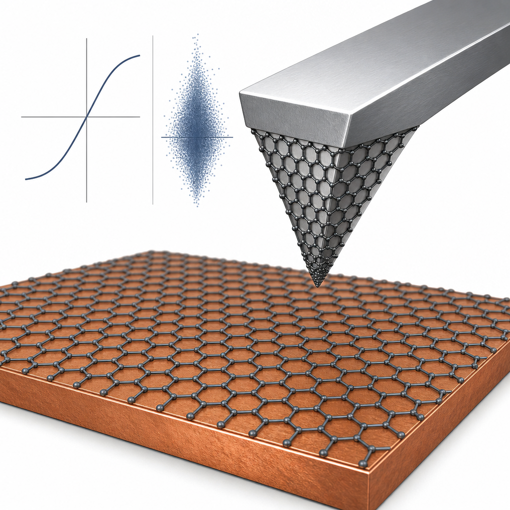
The variability analysis compared statistical distributions of contact resistance and I-V slope across multiple identically prepared graphene-coated tips, as well as across uncoated control tips. Although SEM imaging confirmed that the actual quantity of graphene flakes adhered to each tip varied (a natural consequence of Van der Waals adhesion during ink dipping), the electrical metrics showed that the variability of graphene-coated tips was similar to the variability already present among graphene-free commercial tips of the same model. The graphene coating thus does not introduce additional device-to-device dispersion. Combined with the previously reported lifetime enhancement under high current density and mechanical friction, this places graphene-ink-coated AFM tips on equal footing with bare probes from a reproducibility standpoint while delivering substantially improved durability. The XF013 CVD graphene on copper substrate served as the standard against which these distributions were collected, and Raman/SEM evidence supported the conformal nature of the coating on the apex.
The practical implications extend beyond AFM. The same solution-processed graphene coating workflow could be applied to scanning tunneling microscopy tips, nanoindenter probes, and electrical test pins for semiconductor metrology, all areas where tip lifetime and reproducibility limit throughput. The authors emphasize that, to their knowledge, this is one of the few graphene-based devices whose variability has been quantitatively characterized, and the result clears a major obstacle to commercialization. Future work pointed to by the paper includes scaling the dipping process via batch holders, refining the flake size distribution in the ink, and exploring graphene-coated tips for piezoresponse force microscopy and electrochemical strain microscopy in battery research.
For researchers working on conductive AFM, 2D materials characterization, or printed-electronics device prototyping, this paper illustrates how a well-characterized CVD graphene/Cu reference like the XF013 product available from ACS Material can serve as a reliable benchmark substrate for tip-level electrical testing. The CVD Graphene on Copper Foil category, along with related single-layer graphene films on SiO2, quartz, and PET, is offered for laboratories investigating similar device variability, lifetime, and contact-resistance questions.How ACS Material products were used
- CVD Graphene on Copper Foil (item no. XF013) (CVD Graphene) — “The samples used to test the probes were a piece of conductive SLG grown on copper by CVD (item no. XF013 from ACS Materials)”
Product Performance in this StudyThe ACS Material CVD single-layer graphene on copper served as the reference conductive substrate for collecting tip-to-tip current–voltage curves with graphene-coated AFM probes. Its uniform conductivity enabled the authors to demonstrate that variability among graphene-coated tips was comparable to that of bare tips, validating the AFM-tip coating workflow for commercialization.
Related product categories
Frequently asked questionsWhy is CVD graphene on copper used as a reference substrate for conductive AFM measurements?
CVD-grown single-layer graphene on copper foil offers a highly uniform, atomically flat and electrically conductive surface, which makes it an excellent benchmark for tip-level electrical testing. Because the substrate's contact resistance is essentially constant across the scan area, any variation observed in current–voltage curves can be attributed to differences between AFM probes rather than to the sample, enabling reliable tip-to-tip variability studies.
How does coating an AFM tip with graphene improve its performance?
A conformal graphene coating only a few atomic layers thick protects the tip apex against mechanical wear and electrical degradation under high current densities. Because graphene adds negligible mass and thickness, the cantilever's resonance frequency, spring constant, and tip radius remain essentially unchanged. The result is significantly longer tip lifetime in contact-mode and conductive AFM experiments without compromising spatial or mechanical resolution.
Does graphene-ink coating introduce significant variability between AFM probes?
No. Although the absolute number of graphene flakes attached to each tip varies after dip-coating, statistical comparison of current–voltage curves measured on a common conductive substrate shows that the variability of graphene-coated tips is similar to that already present among uncoated commercial tips. The graphene coating therefore does not add meaningful device-to-device dispersion, supporting commercialization of the technology.