Graphene proved that a single atomic layer could be a remarkable material — but it has one stubborn limitation: no electronic bandgap. That gap is exactly where a whole family of graphene-like two-dimensional materials comes in. Black phosphorus, the transition metal dichalcogenides, MXenes, hexagonal boron nitride, and the elemental “Xenes” share graphene’s atomically thin, layered structure while adding the tunable bandgaps, strong light absorption, metallic conductivity, or insulating behavior that graphene lacks. This guide explains what graphene-like materials are, walks through the major families and what makes each useful, and shows how stacking them into van der Waals heterostructures is reshaping electronics, optoelectronics, energy storage, and sensing.
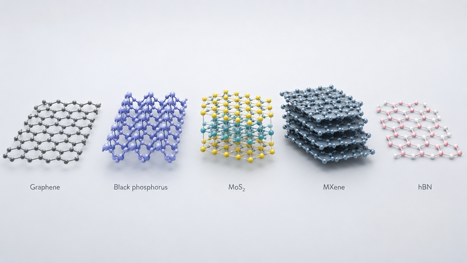
Short answer: “graphene-like materials” are two-dimensional (2D) crystals — one or a few atomic layers thick — that share graphene’s layered, van-der-Waals-bonded structure but have their own distinct electronic properties. The main families are black phosphorus (phosphorene), the transition metal dichalcogenides (TMDs such as MoS2, WS2, MoSe2, WSe2), MXenes (2D metal carbides and nitrides such as Ti3C2), hexagonal boron nitride (hBN), and the elemental Xenes (silicene, borophene, and relatives). Their key advantage over graphene is a tunable, often sizeable bandgap — graphene is a zero-gap semimetal, which makes it a poor switch — so these materials can act as semiconductors (transistors, light emitters), insulators (hBN), or high-conductivity metals (MXenes). Stacked into van der Waals heterostructures, they let researchers build atomically thin devices layer by layer.
The six main graphene-like families at a glance:
| 2D material family | Typical electronic behavior | Key advantage | Common applications |
|---|---|---|---|
| Graphene | Zero-gap semimetal | Very high conductivity and mechanical strength | Transparent electrodes, composites, sensors |
| Black phosphorus (phosphorene) | Direct-gap semiconductor, layer-tunable (~0.3–2 eV) | Tunable direct gap with infrared response | Infrared optoelectronics, field-effect transistors |
| TMDs (e.g. MoS2) | Semiconductors; direct gap as a monolayer (~1.8–1.9 eV) | Strong light emission and switching in monolayers | Transistors, photodetectors, valleytronics |
| MXenes (e.g. Ti3C2) | Metallic / highly conductive | High conductivity plus rich surface chemistry | Energy storage, EMI shielding |
| Hexagonal boron nitride (hBN) | Wide-gap insulator (~6 eV) | Atomically flat, chemically inert dielectric | Substrates, encapsulation, gate dielectrics |
| Xenes (silicene, borophene) | Mostly metallic or semimetallic | Elemental 2D physics, some layer tunability | Research-stage devices |
What does “graphene-like” mean?
When graphene was first isolated in 2004, it showed that a single sheet of atoms could be stable, conductive, and extraordinarily strong.1 The same group soon demonstrated that graphene was not alone: several other layered crystals could be thinned down to one or a few atomic layers, opening up a whole class of two-dimensional (2D) materials.2 These are the “graphene-like” materials — crystals built from atomically thin layers held together by weak van der Waals forces, so they can be peeled apart sheet by sheet just like graphite.
Graphene set an extraordinarily high bar. Its Young’s modulus is near 1 TPa and its intrinsic strength around 130 GPa, making it one of the strongest materials ever measured;3 its thermal conductivity reaches roughly 5000 W/mK;4 and a single layer absorbs about 2.3% of visible light despite being one atom thick.5 What makes graphene-like materials a coherent family is structure, not chemistry: they span elements and compounds — phosphorus, boron, silicon, metal sulfides and carbides — yet all form 2D sheets whose properties change dramatically once thinned to a monolayer. Reviews now catalog dozens of experimentally known 2D materials, with hundreds more predicted by computation.6,7 What unites them, and sets them apart from graphene, is that most are not semimetals — they carry their own bandgaps, light absorption, conductivity, or insulating behavior.
Why look beyond graphene? The bandgap problem
For all its strengths, graphene has one limitation that matters enormously for electronics: it has no bandgap. It is a zero-gap semimetal,1 which means a graphene transistor cannot be switched fully off — there is no energy gap to stop current from flowing. For digital logic, that is a deal-breaker.
This is exactly the niche graphene-like materials fill. Most are semiconductors with a real, and often tunable, bandgap: black phosphorus and the TMDs can be switched on and off like silicon, hBN is a wide-gap insulator, and MXenes are highly conductive metals. Better still, in many of these materials the bandgap changes with the number of layers, with strain, or with an applied field — a design knob that bulk semiconductors simply do not offer. The rest of this guide walks through the major families and what each contributes. For background on graphene itself, see ACS Material’s complete guide to graphene.
Black phosphorus and phosphorene
Black phosphorus (BP) is the most stable allotrope of phosphorus and, like graphite, is layered — its puckered honeycomb sheets can be exfoliated down to a single layer called phosphorene. In 2014, few-layer BP transistors were demonstrated with hole mobilities up to about 1000 cm2/V·s and high on/off ratios,8 and phosphorene was identified as a rare 2D semiconductor combining high mobility with a direct bandgap.9
BP’s standout feature is a thickness-tunable, direct bandgap: roughly 0.3 eV in the bulk, widening to around 2 eV in a single layer.10 That range neatly bridges the gap between graphene (zero) and the larger gaps of the TMDs, making BP especially attractive for infrared optoelectronics. The main practical challenge is stability — bare BP degrades in air as it reacts with oxygen and moisture — so devices are typically encapsulated. Newer work has even produced well-defined phosphorene nanoribbons, extending BP toward edge-controlled electronics.11 ACS Material supplies black phosphorus crystals for this research.
Transition metal dichalcogenides (TMDs)
The transition metal dichalcogenides — compounds of the form MX2, where M is a metal such as Mo or W and X is S, Se, or Te — are the best-studied graphene-like semiconductors. Their defining trick is an indirect-to-direct bandgap crossover: bulk MoS2 is an indirect-gap semiconductor with weak light emission, but a single layer becomes a direct-gap semiconductor (around 1.8–1.9 eV) that emits light strongly, with the gap shifting upward by more than 0.6 eV as the crystal is thinned.12,13
That direct gap makes monolayer TMDs genuine semiconductors. A single-layer MoS2 transistor reached a room-temperature mobility of at least ~200 cm2/V·s with an on/off ratio around 108 — the kind of switching graphene cannot deliver.14 Beyond MoS2, the wider family (MoSe2, WS2, WSe2, and more) has been characterized extensively.15 TMDs also host an extra “valley” degree of freedom: their electrons can be sorted into distinct momentum valleys and selected with circularly polarized light, opening the field of valleytronics.16,17
MXenes: 2D metal carbides and nitrides
MXenes are a younger family, first made in 2011 by selectively etching the aluminium out of a layered ceramic (Ti3AlC2) to leave 2D titanium carbide sheets (Ti3C2).18 The approach generalized quickly: the same etch-and-delaminate route produced a whole series of 2D carbides and nitrides, now numbering around thirty distinct compositions.19
Unlike the semiconducting TMDs, MXenes are typically metallic and exceptionally conductive — among the highest of any solution-processed 2D material — with surfaces rich in functional groups that make them hydrophilic and electrochemically active. That combination has made them stars in energy storage, where 2D titanium carbide delivers very high volumetric capacitance,20 and in electromagnetic interference (EMI) shielding, where thin MXene films outperform far thicker conventional shields.21,22 ACS Material offers an MXene series for researchers.
Hexagonal boron nitride (hBN)
Hexagonal boron nitride is graphene’s structural twin — the same honeycomb lattice, but built from alternating boron and nitrogen atoms instead of carbon. That single substitution turns a conductor into a wide-bandgap insulator (about 6 eV). It makes hBN less of a device channel and more of an enabling material: atomically flat and chemically inert, it is an ideal substrate and dielectric for other 2D materials. Placing graphene on hBN rather than on silicon oxide dramatically improves its electronic quality, raising mobility and reducing disorder.23 Large-area hBN films can now be grown directly, supporting its use as a building block in layered devices.24
The Xenes: silicene, borophene and beyond
The “Xenes” are single-element 2D sheets — the graphene idea applied to other atoms. Silicene, a 2D sheet of silicon, was confirmed experimentally in 2012; unlike flat graphene it adopts a gently buckled honeycomb, yet keeps graphene-like Dirac electronic behavior, with the bonus of stronger spin-orbit coupling and natural compatibility with silicon electronics.25 Borophene, a 2D sheet of boron, was synthesized in 2015 on a silver surface; it is a highly anisotropic metal whose properties depend strongly on direction.26 Other members — germanene, stanene, and more — extend the family further. Most Xenes are not yet stable in air on their own, so they remain largely a research frontier, but they round out the picture of just how general the 2D concept has become.
The tunable-bandgap advantage
The single most important way graphene-like materials differ from graphene — and from one another — is the bandgap. The interactive below places the families on a common bandgap scale, from metals through semiconductors to insulators, and shows how a material like MoS2 or black phosphorus shifts its gap as layers are added or removed.
What the simulator shows. Model: a material’s electronic bandgap determines whether it behaves as a metal (no gap), a semiconductor (a moderate gap that can be switched on and off), or an insulator (a large gap). Graphene sits at zero — a semimetal. Black phosphorus spans roughly 0.3 eV (bulk) to ~2 eV (monolayer);10 monolayer MoS2 is a direct-gap semiconductor near 1.8–1.9 eV, up from an indirect ~1.2 eV in the bulk;12,13 and hexagonal boron nitride sits far to the right as a ~6 eV insulator. Takeaway: this tunability — by material choice and by layer number — is the design freedom that graphene’s fixed zero gap cannot provide. Values are representative figures from the cited studies; exact gaps depend on layer count, strain, substrate, and measurement method.
How graphene-like materials are made
Two broad routes dominate. Top-down exfoliation peels layers from a bulk crystal — either mechanically (the “Scotch-tape” method that first isolated graphene) or in liquid, where sonication in the right solvent splits layered crystals into 2D nanosheets in scalable quantities.27 Bottom-up growth builds the sheets atom by atom, most commonly by chemical vapor deposition (CVD) for large-area films, or by molecular beam epitaxy for the more delicate Xenes. MXenes use a different, chemistry-driven route entirely: selectively etching one element out of a layered parent crystal.18 The right method depends on the material and the application — research often needs small, high-quality flakes, while devices need large, uniform films.
Van der Waals heterostructures
Because 2D layers are held together only by weak van der Waals forces, different materials can be stacked on top of one another without the lattice-matching constraints that limit conventional semiconductors. The result is the van der Waals heterostructure: a deliberate stack of dissimilar 2D sheets — a conductor here, a semiconductor there, an insulator in between — assembled almost like atomic-scale Lego.28,29 These stacks are where the families come together: hBN insulates and protects, TMDs provide the active semiconductor, graphene supplies transparent electrodes, and the interfaces themselves can host new physics. Working devices already exist — for example, vertical transistors built from graphene–WS2 stacks for flexible, transparent electronics.30
Applications
Taken together, graphene-like materials cover a remarkable span of uses:
- Electronics. TMDs and black phosphorus provide the switchable semiconductors graphene lacks, for atomically thin transistors.8,14
- Optoelectronics. Direct-gap monolayer TMDs emit and detect light efficiently, and black phosphorus extends this into the infrared.12,10
- Energy storage. Conductive MXenes serve as high-capacitance electrodes for batteries and supercapacitors.20,21
- EMI shielding and coatings. Thin MXene films block electromagnetic interference far better than their thickness would suggest.22
- Substrates and dielectrics. hBN underpins high-performance 2D devices as an atomically flat insulator.23
- Valleytronics and quantum technologies. The valley degree of freedom in TMDs points toward entirely new device concepts.16,17
ACS Material graphene-like materials
- Graphene-Like Materials — the full catalog of 2D materials beyond graphene.
- Black Phosphorus — layered BP crystals for exfoliation into phosphorene.
- MXene Series — 2D titanium carbide and related MXenes.
- Graphyne Series — carbon-allotrope 2D materials related to graphene.
- Graphene Series — graphene, graphene oxide, and rGO grades.
Explore ACS Material’s full range of graphene-like 2D materials — black phosphorus, MXenes, graphyne-related materials, and graphene grades — for your next 2D-materials project.
Frequently asked questions
What are graphene-like materials?
They are two-dimensional crystals — one or a few atoms thick — that share graphene’s layered, van-der-Waals-bonded structure but have their own electronic properties. The main families are black phosphorus, the transition metal dichalcogenides, MXenes, hexagonal boron nitride, and the elemental Xenes.
How are they different from graphene?
Graphene is a zero-gap semimetal, so it cannot be switched fully off. Most graphene-like materials have a real, often tunable, bandgap, which lets them act as semiconductors, insulators, or highly conductive metals depending on the material.
Which graphene-like material is the most important?
It depends on the application: the TMDs (such as MoS2) for semiconductor electronics and optoelectronics, MXenes for energy storage and EMI shielding, hexagonal boron nitride for substrates and dielectrics, and black phosphorus for infrared optoelectronics.
Do graphene-like materials have a bandgap?
Yes — most do, unlike graphene. In many of them the gap depends on the number of layers, so it can be tuned by thinning the crystal down toward a monolayer.
What is a van der Waals heterostructure?
It is a stack of different 2D materials held together by van der Waals forces, assembled to combine their properties — for example an insulating hBN layer, a semiconducting TMD, and a graphene electrode in one device.
Are graphene-like materials stable in air?
It varies. TMDs and hexagonal boron nitride are quite stable, whereas black phosphorus and most Xenes degrade in air and usually need encapsulation for device work.
References
This article is provided by ACS Material LLC for educational purposes and describes graphene-like two-dimensional materials, including black phosphorus, transition metal dichalcogenides, MXenes, hexagonal boron nitride, and the elemental Xenes. Property figures cited from the referenced studies — such as bandgaps, carrier mobilities, thermal conductivity, and mechanical strength — were obtained under specific experimental conditions and depend strongly on layer number, strain, substrate, encapsulation, and measurement method; real-world values will differ. The interactive bandgap chart is a schematic teaching tool based on representative values from the cited literature and is not a database of exact material parameters. Consult product datasheets and safety data sheets for grade-specific specifications and handling guidance.