-
Graphene-Shielded SERS Substrate - Zhejiang University, 2015
Jul 07, 2026 | ACS MATERIAL LLCLiu, X. et al. (2015). Compact Shielding of Graphene Monolayer Leads to Extraordinary SERS-Active Substrate with Large-Area Uniformity and Long-Term Stability. *Scientific Reports*. https://doi.org/10.1038/srep17167
Scientific Reports · 2015
Zhejiang University researchers use CVD monolayer graphene to shield periodic metallic SERS substrates, delivering uniform, stable, high-sensitivity Raman sensing.
About this research
Researchers at Zhejiang University used CVD-grown monolayer graphene to encapsulate a periodic metallic nanostructure, producing a surface-enhanced Raman scattering (SERS) substrate with large-area uniformity and long-term operational stability. Published in Scientific Reports (2015), the work demonstrates that a single atomic layer of graphene is sufficient to shield silver/gold plasmonic features from oxidation and contamination while preserving — and in some cases enhancing — the SERS signal. The team further patterned the graphene-shielded surface into a sensing-spot array, pointing toward practical, reproducible high-throughput Raman analysis.
SERS is one of the most sensitive vibrational spectroscopy techniques available, in principle reaching single-molecule detection through localized surface plasmon resonance in metallic nanostructures. In practice, however, adoption has been hindered by the difficulty of producing SERS substrates that are simultaneously uniform across large areas, reproducible between batches, and stable over time. Lithography can deliver ordered hotspots but is expensive and slow; roughened electrodes and colloidal nanoparticles are cheap but variable; and noble metal surfaces invariably suffer oxidation, sulfidation, and carbon contamination that degrade the plasmonic response. A robust, scalable passivation strategy is therefore a long-standing need in plasmonic sensing, food safety screening, trace pollutant detection, and biomedical diagnostics.
The authors fabricated a periodic metallic nanostructure and then transferred a continuous monolayer of CVD graphene over the entire active surface. CVD graphene grown on copper foil is industrially available at wafer scale, has uniform sub-nanometre thickness, is mechanically strong, chemically inert, and impermeable to most gases and liquids. These properties make it an ideal compact shielding layer: it sits within the decay length of the plasmonic near-field so that analyte molecules adsorbed on top still experience strong electromagnetic enhancement, yet it physically separates the metal from corrosive ambient species. The graphene also provides a uniform, π-conjugated adsorption surface that binds aromatic analytes through π–π stacking, improving capture of molecules that interact only weakly with bare noble-metal surfaces. The same fabrication route was extended to define arrays of discrete graphene-shielded SERS sensing spots for multiplexed analysis.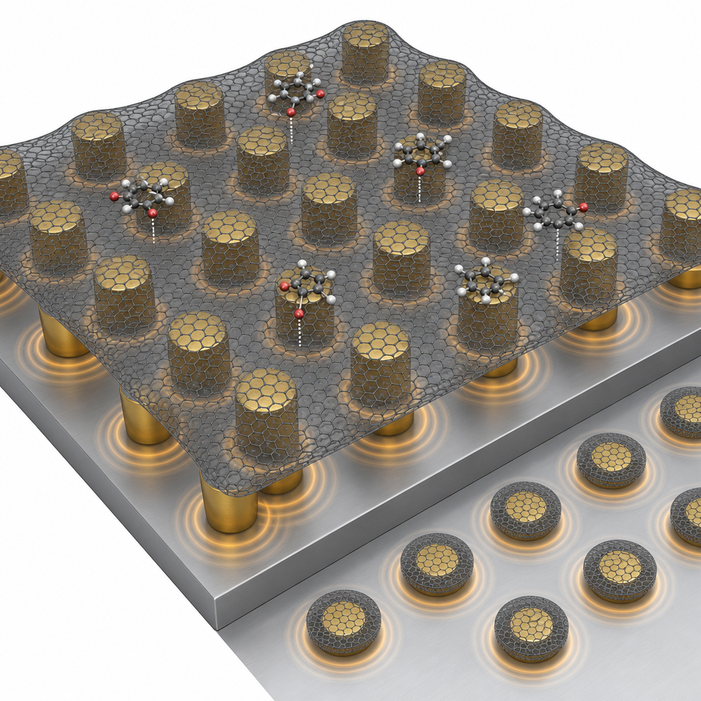
The shielded substrate exhibited markedly enhanced physical and chemical stability compared with unshielded controls. Whereas conventional metallic SERS substrates degrade through oxidation, corrosion, and morphological change — all of which alter the localized surface plasmon resonance and suppress signal — the graphene-capped substrate retained its SERS activity over extended storage and repeated use. Photo-induced damage of adsorbed molecules under laser illumination was alleviated, because the graphene layer dissipates heat and quenches reactive species at the metal–analyte interface. Importantly, the enhancement factor of the substrate was preserved, and for certain analytes that adsorb only weakly on bare metal, sensitivity actually improved due to graphene-mediated affinity. The patterned sensing-spot arrays produced spot-to-spot reproducibility consistent with the requirements of quantitative high-throughput analysis, in contrast to the substantial variability typical of nanoparticle-based SERS platforms.
Applications span any field where reliable, quantitative Raman detection is needed: trace contaminant screening in food and water, point-of-care biomedical diagnostics, environmental monitoring of pesticides and dyes, and combinatorial screening in chemistry. The graphene-shielded architecture also opens fundamental studies of SERS by providing a chemically stable, well-defined surface on which to systematically compare analytes and excitation conditions. The authors highlight that the array format makes the platform compatible with multi-analyte sensing chips and automated readout. Follow-on work could integrate the substrate with microfluidics, explore alternative 2D shielding layers such as hexagonal boron nitride, or combine plasmonic hotspots with functionalized graphene to selectively bind specific target classes.
For researchers building similar plasmonic or 2D-material sensing platforms, the same class of CVD monolayer graphene on copper foil used in this study is available from ACS Material, along with related CVD graphene on SiO2, quartz, and PET substrates, and trivial-transfer graphene films for direct lamination onto pre-patterned metallic nanostructures. The paper underscores that a single graphene monolayer, properly integrated, can address two of the most persistent limitations of SERS in one step.How ACS Material products were used
- CVD Graphene on Copper Foil (CVD Graphene) — “the industrial-scale graphene film grown by chemical vapor deposition (CVD) are widely available”
Product Performance in this StudyThe CVD monolayer graphene served as a chemically inert, impermeable shielding layer over the periodic metallic nanostructure, preserving SERS activity while drastically improving long-term stability and uniformity, and even enhancing detection sensitivity for weakly-adsorbed analytes.
Related product categories
Frequently asked questionsHow does monolayer graphene improve SERS substrate stability?
Monolayer graphene is chemically inert, mechanically strong, and impermeable to most gases and liquids. When transferred onto a metallic SERS substrate, it acts as a compact corrosion barrier that prevents oxidation, sulfidation, and contamination of the underlying plasmonic metal. Because graphene is only one atom thick, the analyte still sits within the plasmonic near-field, so the SERS enhancement is preserved while substrate lifetime and reproducibility increase dramatically.
Why use CVD graphene rather than exfoliated graphene for SERS shielding?
CVD graphene grown on copper foil can be produced at wafer scale with uniform monolayer thickness and continuous coverage, which is essential for shielding a large-area periodic SERS substrate. Mechanically exfoliated flakes are too small and irregular for practical sensor arrays. CVD graphene also transfers cleanly onto pre-patterned plasmonic structures, enabling reproducible fabrication of identical sensing spots suitable for high-throughput quantitative Raman analysis.
Does the graphene layer reduce SERS sensitivity for analyte detection?
No. The graphene is only ~0.34 nm thick, so analyte molecules remain within the decay length of the plasmonic near-field and still experience strong electromagnetic enhancement. For molecules that adsorb only weakly to bare noble metals, sensitivity actually improves because graphene's π-conjugated surface captures aromatic analytes through π–π stacking, concentrating them at the hotspots while simultaneously suppressing photo-induced sample damage.