-
Graphene Thermal Emitter Metamaterial - University of Exeter, 2018
Jun 08, 2026 | ACS MATERIAL LLCShi, C. et al. (2018). Metamaterial-based graphene thermal emitter. *Nano Research*.
Nano Research · 2018
University of Exeter researchers built a dual-band mid-infrared graphene thermal emitter using ACS Material multilayer graphene and h-BN encapsulation.
About this research
Researchers at the University of Exeter demonstrated a metamaterial-based mid-infrared thermal emitter built around multilayer graphene supplied by ACS Material, achieving tailored dual-band emission at approximately 4.2 μm and 7 μm. The team combined a hexagonal boron nitride (h-BN) encapsulated multilayer graphene filament (6-8 layers) with a gold concentric-ring-resonator frequency-selective surface (FSS), reshaping the broadband gray-body radiation of a Joule-heated graphene strip into two narrow bands aligned with the CO2 absorption window and a nearby transparent reference window. Published in Nano Research (2018), the work shows that an inexpensive incandescent-style emitter can rival semiconductor mid-IR LEDs in spectral selectivity while operating in ambient air at sub-millisecond modulation speeds.
Mid-infrared (2-20 μm) sources are essential for molecular spectroscopy, gas sensing, security imaging and astronomical observation, because most functional groups have characteristic vibrational fingerprints in this band. The available source technologies all involve trade-offs: bandgap LEDs modulate fast but emit weakly; interband and quantum cascade lasers are powerful but require complex epitaxy and high cost; and conventional incandescent emitters (tungsten coils, micromachined silicon membranes) are bright and cheap but slow and spectrally broad, forcing the use of choppers and bandpass filters. A graphene filament, with its extreme breakdown current density, high thermal conductivity, low thermal mass and demonstrated stability when h-BN-encapsulated, offers a path to combine the brightness of an incandescent source with sub-millisecond switching - and, when paired with a planar metamaterial, with narrowband spectral output.
Multilayer graphene from ACS Material formed the active emitting filament of the device. The authors specifically state that a 6-8 layer graphene sample obtained from ACS Material was used because it is readily available from suppliers and provides a relatively high emissivity compared with monolayer graphene. The graphene was patterned into a filament, contacted with gold electrodes for current injection, and fully encapsulated in h-BN films. The h-BN layers electrically and thermally isolate the graphene from the FSS metamaterial layer on top and from the 500 μm highly doped silicon substrate (with a 300 nm thermal oxide) below, while also enabling sustained operation in air. On the upper h-BN surface, Cr/Au (5/50 nm) concentric ring resonators were patterned by direct-write electron beam lithography in a 2 × 2 unit-cell arrangement, with the larger rings (r2 = 400 nm) on the diagonal and smaller rings (r1 = 200 nm) off-diagonal, a 3.6 μm period, and ring widths of 200 nm. The device was divided into four 250 μm × 250 μm quadrants, two with rings and two without, enabling direct on-chip comparison of emission with and without the metamaterial.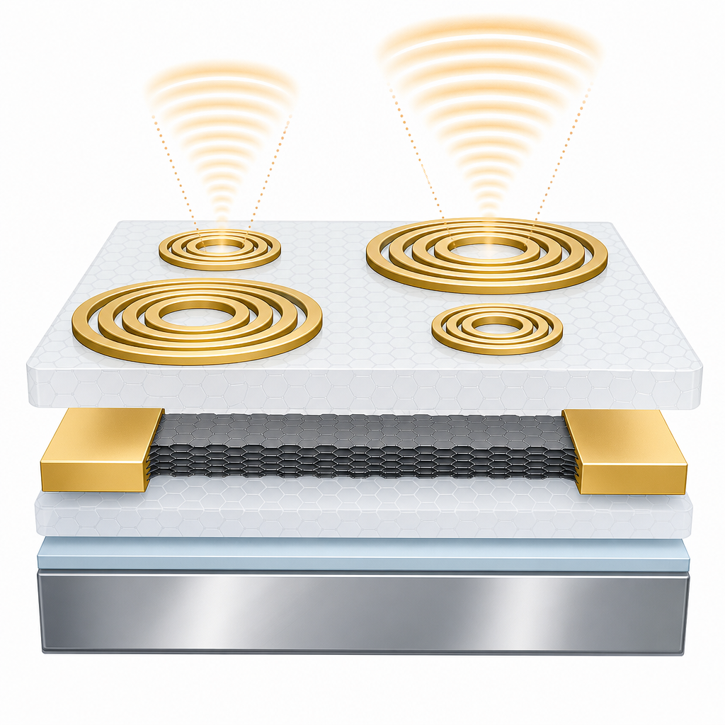
Finite-difference time-domain simulations using a Kubo-formula 2D Ohmic-sheet model for graphene predicted two emission peaks, and these were confirmed experimentally with a Fourier-transform infrared spectrometer. Reflection spectra recorded with a 40× reflecting objective showed two pronounced minima at 4.2 μm and 7 μm, matching the calculated resonances of the small and large rings respectively, with a characteristic "W"-shaped response. Emission measurements with the filament driven by a 1 kHz, 50% duty-cycle square wave at 50 mA peak current produced a two-peak spectrum that closely tracked the simulated profile. Spatial mapping confirmed that the metamaterial quadrants reflected more and emitted differently than the bare-graphene quadrants, consistent with Kirchhoff's law. Atmospheric CO2 (4.3 μm) and water vapor (7.3 μm) features were visible in the measured spectra. Simulations further showed that replacing the silicon substrate with a more conductive layer (e.g., gold) turns the oxide spacer into an underdamped resonant cavity, lifting the quality factor of the emission peaks to approximately Q ≈ 8.3 - more than twice that of typical commercial mid-IR LEDs - while concentrating emission into two sharper bands at 6.3 μm and 4.3 μm.
The most direct application is non-dispersive infrared (NDIR) gas sensing: by tuning the ring geometry, one emission band can be placed on a target gas absorption (CO2, hydrocarbons, water vapor, NOx) and the other on a nearby reference wavelength, eliminating the need for external optical filters and mechanical choppers. The high modulation speeds compatible with graphene thermal emitters open the door to lock-in detection schemes and compact, low-power sensor modules for indoor air quality, automotive emissions, breath analysis and industrial process monitoring. Because the spectral peaks are set lithographically rather than by epitaxial bandgap engineering, the same platform can be reconfigured for many gases, and the architecture is compatible with silicon-foundry processing, suggesting a cost-effective route to scalable mid-infrared photonic devices.
For researchers developing graphene-based optoelectronics, infrared emitters, or 2D-material heterostructures, the choice of starting graphene matters: emissivity, uniformity and electrical robustness directly determine device performance. ACS Material's multilayer graphene and related CVD graphene and h-BN products are well-suited to this kind of work, providing the few-layer films and transferable membranes needed to build encapsulated filaments and metamaterial-integrated devices. This study illustrates how a commercially available graphene starting material, combined with conventional lithographic patterning, can deliver mid-infrared emitter performance that begins to challenge much more elaborate semiconductor sources.How ACS Material products were used
- Multilayer graphene (6-8 layers) (Graphene Series) — “Ring resonators, consisting of 5/50 nm-thick Cr/Au, were patterned on the top boron nitride layers of an encapsulated multilayer graphene filament (6-8 layers, obtained from ACS Material) using direct-writing electron beam lithography.”
Product Performance in this StudyThe 6-8 layer graphene from ACS Material served as the incandescent emitting filament. Its high emissivity, mechanical strength, high breakdown current density and low thermal mass enabled stable mid-infrared emission with high modulation speed when Joule-heated.
Related product categories
Frequently asked questionsWhy use multilayer graphene rather than monolayer for a thermal emitter?
Multilayer graphene (6-8 layers in this work) provides significantly higher infrared emissivity than monolayer graphene while keeping the thermal mass low enough for sub-millisecond modulation. It is also more readily available from commercial suppliers and is mechanically robust enough to be patterned, contacted, and h-BN encapsulated without degrading. The result is a brighter mid-infrared incandescent filament that still switches much faster than a tungsten coil.
How does hexagonal boron nitride encapsulation improve graphene emitters?
Hexagonal boron nitride layers above and below the graphene filament electrically and thermally isolate it from the metamaterial and substrate, preserve the graphene's electronic quality, and crucially protect it from oxidation. This allows the filament to operate stably in ambient air at high temperatures, which a bare graphene strip cannot. The h-BN also provides a flat, insulating platform for lithographically defining the ring-resonator metamaterial on top.
What determines the emission wavelengths of a metamaterial graphene emitter?
Emission peaks are set by the geometry of the metallic ring resonators on the device surface, not by an electronic bandgap. In this study, rings with radii of 200 nm and 400 nm and a 3.6 μm unit-cell period produced peaks near 4.2 μm and 7 μm. Changing the inner/outer radius, ring width, or periodicity shifts the resonances, allowing the same platform to be tuned to any target absorption line in the 2-20 μm mid-infrared range.