-
Hexagonal Boron Nitride
Sep 06, 2018 | ACS MATERIAL LLCHexagonal Boron Nitride (h-BN) has recently gained strong interest as a strategic component in engineering Van der Waals heterostructures with two dimensional crystals such as graphene. h-BN film can be synthesized by chemical vapor deposition (CVD) on catalytic substrates and the atomic layers can be controlled by changing the precursors, growth time and cooling rates etc. The unique properties of h-BN film offer promising potential in physical, mechanical, optical, electronic and hybrid applications.
Introduction
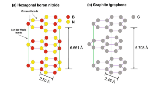
Boron Nitride (BN) is a typical III-V group compound with a stoichiometry of boron to nitrogen of 1:1. BN can be isomorphic to carbon in any lattice structure from zero-dimensional (0D) cage, one-dimensional (1D) nanotube, two-dimensional (2D) monolayer to three dimensional (3D) diamond-like crystal structures.1, 2 Hexagonal boron nitride (h-BN) is a 2D insulator with a wide bandgap (>6eV) and an atomic structure very similar to that of graphene where boron and nitrogen atoms alternate at the vertices of a planar hexagonal sp2 network (Figure 1). A number of exceptional properties and immense potential for diverse applications makes 2D hexagonal BN (h-BN) very popular. Various methods such as mechanical and chemical exfoliation have been developed to fabricate 2D h-BN.4.5 However, the aforementioned methods produce h-BN flakes non-uniform in thickness. Consequently, h-BN films with uniform thickness and precise control over the number of layers have gained increased popularity.

Figure 1. Crystal structures of (a) hexagonal
boron nitride and (b) graphite/graphene.3Synthesis
Chemical vapor deposition (CVD) on catalytic substrates has been widely adopted to grow large area h-BN film.6 The size of the sample is determined by the substrate size. The precursor can be gas (diborane and ammonia),7 liquid (borazine)8 and solid9(ammonia borane). Various parameters of h-BN film such as grain size control, grain morphology control, grain orientation control, layer number control have been investigated with intensive research efforts.

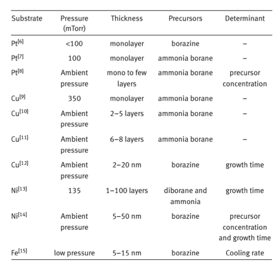
Table 1. Summary of factors in relation with the layer number of
obtained h-BN. 3Table 1 summarizes the factors influencing the synthesis of h-BN film. Pt, Cu, Ni and Fe have been used as substrates. The h-BN domain size can also be enlarged by improving the surface flatness, which is realized by electropolishing and a long pre-annealing treatment of the substrate. Thus, the properties of the substrate affect the domain size of h-BN greatly.
The layer number of h-BN film is very important for its practical applications in electrical devices. From Table 1, the layer number of h-BN grown on the substrate is sensitive to the chamber pressure. Low pressure CVD growth mainly gives rise to monolayer h-BN and ambient pressure CVD growth results in few layers (Table 1). Pressure dependence on layer numbers of h-BN continues to be under investigation. It is thought that diffusion length and concentration of the precursor on the metal surface play an important role.
Other methods for fabrication of large area h-BN film are continually being researched. For example, ion beam supporting deposition has been utilized to grow h-BN on Cu foil. Physical vapor deposition is another scalable method to produce few-layer h-BN film with uniform thickness.
In practical applications transferring h-BN film from the metal substrates on which they are synthesized to other substrates is necessary. We followed a typical procedure to transfer h-BN to arbitrary substrates for further characterization. The transfer procedure is as follows: spin-coating thin poly methyl methacrylate (PMMA) film onto the surface of h-BN/metal, etching the underlying metal such as Cu, Ni, Pt to release the flexible PMMA/h-BN film into diluted HCl and FeCl3 (0.5 mol.L-1) aqueous solution, placing the PMMA/h-BN film onto target substrates, and finally dissolving the thin PMMA layer with acetone.
Applications
h-BN possesses many advantageous properties including excellent stability, high thermal conductivity, electrical insulation, high elastic modulus and low friction coefficient, making it attractive for many fields of applications. The excellent thermal and chemical stability of h-BN makes it great for serving as a multifunctional coating material, for instance. 2D h-BN can be stable in temperatures as high as 1,500 °C in air and will not react with most chemicals, therefore it can be used to create a chemically stable, high-temperature and oxidation-resistant coating.
Exfoliated h-BN sheets have shown promising oxidation protection for ferromagnetic contacts in spintronic devices and unstable 2D material channels including black phosphorus and niobium diselenide as examples. As a wide band gap semiconductor with ultraviolet luminescence, h-BN has been proposed as a detector for photon emission, ultraviolet and deep ultraviolet (DUV). Investigations of other possible applications of h-BN are ongoing.
Conclusion
Large scale h-BN film with controllable atomic layers have been synthesized by CVD method, but still confront some challenges. Especially for commercial applications, new methods to synthesize high-quality and large-size h-BN films with controlled thicknesses are still required. Control of the surface roughness of the substrate is another crucial factor because a single atomic layer of BN is strongly influenced by the substrate morphology. h-BN films exhibit promising potential for applications in various fields.
ACS Material Products:
Trivial Transfer Hexagonal Boron Nitride (TTh-BN)
Hexagonal Boron Nitride (H-BN) On Copper Foil
Hexagonal Boron Nitride (H-BN) On Si/SiO2
References
1. Pease R S. Crystal structure of boron nitride. Nature, 1950, 165 (4201): 722-723.
2. Jun Y, Ji dong L, Hang Y, Jin Y, Guoan T, Xuemei L, Zhuhua Z, Wanlin G. Boron Nitride Nanostructures: Fabrication, Functionalization and Applications. Small, 2016, 12 (22): 2942-2968.
3. Kim K K, Kim S M, Lee Y H. A New Horizon for Hexagonal Boron Nitride Film. Journal of the Korean Physical Society, 2014, 64 (10): 1605-1616.
4. Gorbachev R V, RiazI, Nair R R, Jalil R, Britnell L, Belle B D, HillE W, NovoselovK S, Watanabe K, Taniguchi T, Geim A K, Blake P. Hunting for monolayer boron nitride: optical and Raman sinatures. Small, 2011, 7, 465-468.
5. Pacilé D, Meyer J C, Girit Ç Ö, Zettl A. Direct growth of graphene on in situ epitaxial hexagonal boron nitride flakes by plasma-assisted molecular beam epitaxy. Applied Physics Letters, 2008, 92, 133107.
6. Kim K K, Hsu A, Jia X, Kim S M, Shi Y, Hofmann M, Nezich D, Rodriguez-Nieva J F, Dresselhaus M, Palacios T, Kong J. Synthesis of Monolayer Hexagonal Boron Nitride on Cu Foil Using Chemical Vapor Deposition. Nano
Letters, 2012, 12(1):161-166.7. Ismach A, Chou H, Ferrer D A, Wu Y, McDonnell S, Floresca H C, Covacevich A, Pope C, Piner R, Kim M J, Wallace R M, Colombo L, Ruoff R S. Toward the controlled synthesis of hexagonal boron nitride films. ACS Nano, 2012, 6 (7):6378-6385.
8. Kim K K, Hsu A, Jia X, Kim S M, Shi Y, Dresselhaus M,Palacios T, Kong J. Synthesis and characterization of hexagonal boron nitride film as a dielectric layer for graphene devices.ACS Nano, 2012, 6(10):8583-8590.
9. Shi Y, Hamsen C, Jia X, Kim K K, Reina A, Hofmann M, Hsu A L, Zhang K, Li H, Juang Z Y, Dresselhaus M S, Li L J,Kong J. Synthesis of few-layer hexagonal boron nitride thin film by chemical vapor deposition. Nano Letters, 2010, 10 (10): 4134-4139.
10. Kim S M, Hsu A, Park M H, Chae S H, Yun S J, Lee J S, Cho D H, Fang W, Lee C, Palacios T, Dresselhaus M, Kim K K, Lee Y H, Kong J. Synthesis of large-area multilayer hexagonal boron nitride for high material performance. Nature Communications, 2015, 6, 8662.