-
Monolayer Graphene 99% NIR Absorber - NUDT, 2016
Jun 16, 2026 | ACS MATERIAL LLCGuo, C. et al. (2016). Experimental Demonstration of Total Absorption over 99% in the Near Infrared for Monolayer‐Graphene‐Based Subwavelength Structures. *Advanced Optical Materials*. https://doi.org/10.1002/adom.201600481
College of Optoelectronic Science and Engineering National University of Defense Technology Changsha Hunan 410073 China · Advanced Optical Materials · 2016
Researchers at National University of Defense Technology used ACS Material monolayer graphene to demonstrate over 99% near-infrared absorption at 1.5 μm.
About this research
Researchers at the College of Optoelectronic Science and Engineering National University of Defense Technology Changsha Hunan 410073 China used ACS Material monolayer graphene to experimentally demonstrate peak optical absorption of over 99% near 1.5 μm in the near-infrared, the first direct experimental realization of near-complete absorption in a monolayer-graphene-based subwavelength structure. The device sandwiches a single sheet of CVD graphene between a one-dimensional PMMA grating and a silica layer backed by a gold mirror, and the measured spectra match finite-element simulations almost perfectly. The 19–20 nm full-width-at-half-maximum resonance confirms that careful resonant engineering can lift graphene's intrinsic 2.3% absorption to the limit of complete absorption.
The ability to make a single atomic layer of carbon absorb essentially all incident near-infrared light addresses a central bottleneck for graphene optoelectronics. Although graphene offers ultrafast response, broadband coverage from UV to terahertz, and ultrahigh carrier mobility, suspended monolayer graphene absorbs only 2.3% of normally incident light, which limits photodetector responsivity, modulator depth, and photovoltaic conversion. Previous experiments using 1D dielectric gratings or 2D silicon photonic crystals on back-mirror geometries reached only ~40%, ~77%, or ~85% absorption. Pushing experimental absorption past 99% means that graphene can now realistically compete with bulk semiconductor absorbers in the 1.5 μm telecommunications window, with implications for on-chip photodetectors, optical modulators, narrowband filters, infrared sensors, and thermal emitters.
The ACS Material monolayer graphene was the active light-absorbing element of the entire device, and its quality was critical to the result. Fabrication began on a 2 cm silicon substrate with electron-beam evaporation of a 4 nm chromium adhesion layer followed by magnetron sputtering of a 200 nm gold reflector. A 520 nm silica spacer was then deposited by plasma-enhanced chemical vapor deposition. A 1 cm piece of monolayer graphene from ACS Material was transferred onto the silica spacer, and PMMA was spin-coated on top and patterned by electron-beam lithography into 1D subwavelength gratings of varying period. The authors recorded Raman spectra of the graphene as supplied by ACS Material and again after the full lithographic process. The post-fabrication spectrum showed essentially no D peak around 1350 cm⁻¹ and was nearly identical to the pristine spectrum, confirming that the starting graphene was of high crystalline quality and that this quality survived deposition, transfer, and lithography. This is what allowed the resonant cavity to reach the critical-coupling condition required for total absorption.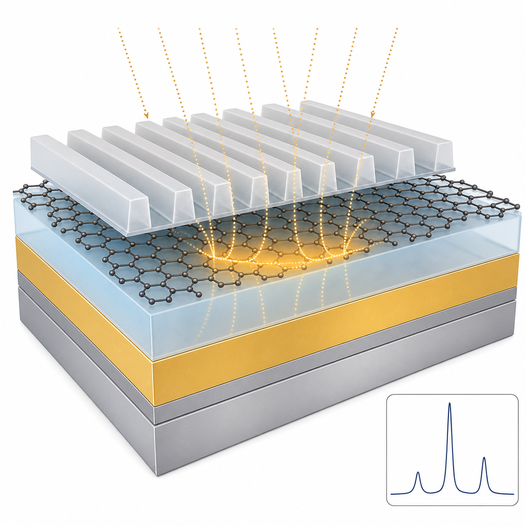
Quantitatively, the structure with grating period d = 1254 nm exhibited measured peak absorption above 98% for transverse-electric polarization, with a measured FWHM of 19 nm at the OSA resolution of 2 nm. Simulation predicted peak absorption above 99% at wavelengths around 1.5 μm with FWHM near 20 nm, and the measured curve overlays the simulated curve almost identically across the resonance and its sidebands. Reflection spectra were calibrated against the 200 nm gold layer in the same sample, assumed to be 98.8% reflective at 1500 nm based on simulation, and absorption was extracted as A = 1 − R because the gold layer fully blocks transmission. By varying the grating period the team tuned the resonant absorption wavelength continuously across the near-infrared while preserving the high peak absorption. For transverse-magnetic polarization no resonant mode appeared in this wavelength range, so absorption stayed low; the authors note that patterning a 2D array in the PMMA layer would make the response polarization-independent.
Applications follow directly from the result. A monolayer absorber with >99% absorption and a ~20 nm linewidth tuned by a simple PMMA grating is attractive for narrowband near-infrared photodetectors, electro-absorption modulators at 1550 nm, hyperspectral imaging pixels, infrared filters, and thermal emitters. Because the graphene retains its native ultrafast carrier dynamics, such structures can in principle combine record absorption with picosecond response. The authors point to 2D grating patterning to remove polarization dependence as the natural next step, and the same low-index-contrast resonant strategy can be extended to other 2D materials such as MoS2, WS2, and black phosphorus for absorbers across the visible and short-wave infrared.
For researchers building graphene optoelectronic devices, the work demonstrates that commercially supplied monolayer CVD graphene, when handled with standard transfer and lithography, is good enough to reach the theoretical limit of resonant absorption. The CVD monolayer graphene used here is available from ACS Material in formats including graphene on copper foil and graphene transferred onto SiO2, quartz, or PET substrates, making it directly applicable to groups working on photodetectors, modulators, plasmonic devices, and 2D-material photonics.How ACS Material products were used
- CVD Monolayer Graphene (transferred onto silica/gold/silicon substrate) (CVD Graphene) — “a 1 cm size monolayer graphene (ACS MATERIAL) was transferred on the top of the silica layer”
Product Performance in this StudyThe ACS Material monolayer graphene functioned as the sole absorbing layer in the subwavelength resonant structure. Raman comparison before and after fabrication showed no D peak, confirming that the as-received graphene quality was preserved through device fabrication, enabling >99% peak absorption near 1.5 μm.
Related product categories
Frequently asked questionsHow can monolayer graphene absorb more than 99% of near-infrared light?
Suspended monolayer graphene absorbs only 2.3% of normally incident light. Coupling it to a resonant cavity, in this case a PMMA subwavelength grating on top of a 520 nm silica spacer and a 200 nm gold back mirror, traps light at the graphene plane through guided-mode resonance and critical coupling. When the reflected wave destructively interferes with the resonant re-emission, transmission is blocked by gold and absorption approaches unity, exceeding 99% at 1.5 μm.
Why is high-quality CVD monolayer graphene important for resonant near-infrared absorbers?
Critical coupling requires the graphene loss to match the cavity leakage rate, and excess defects broaden the resonance and lower peak absorption. Raman characterization in this study showed essentially no D peak before or after device fabrication, confirming that the ACS Material monolayer graphene preserved its crystalline quality through transfer, PECVD silica deposition, spin coating, and electron-beam lithography, which was necessary to reach the >99% absorption demonstrated experimentally.
What applications benefit from total absorption in monolayer graphene at 1.5 μm?
A monolayer absorber that captures over 99% of light at the 1550 nm telecom wavelength with a narrow 20 nm linewidth is directly useful for near-infrared photodetectors, electro-absorption modulators, narrowband filters, hyperspectral imaging pixels, and thermal emitters. Because graphene retains picosecond carrier dynamics, such resonant absorbers can combine high absorption with ultrafast response, addressing a long-standing limitation of graphene optoelectronic devices.