-
Nanopatterned Graphene FET via BCP Lithography — UC San Diego, 2014
Jun 09, 2026 | ACS MATERIAL LLCChoi, D. et al. (2014). Nanopatterned graphene field effect transistor fabricated using block co-polymer lithography. *Materials Research Letters*. https://doi.org/10.1080/21663831.2013.876676
Materials Research Letters · 2014
UC San Diego used ACS Material CVD single-layer graphene to fabricate nanopatterned graphene FETs with ~19 nm necks and a ~0.08 eV bandgap.
About this research
Researchers at the University of California, San Diego used CVD single-layer graphene purchased from ACS Material to fabricate nanopatterned graphene (NPG) field-effect transistors (FETs) using block co-polymer (BCP) lithography with poly(styrene-b-4-vinylpyridine) (PS-b-P4VP), producing a homogeneous nanomesh with ~19 nm neck widths and a measured bandgap opening of ~0.08 eV. The study, published in Materials Research Letters (2014), is the first demonstrated use of PS-b-P4VP for graphene nanopatterning and shows that a scalable, self-assembled polymer template can replace expensive e-beam lithography for sub-20 nm feature definition in 2D materials. Both single-layer and few-layer NPG FETs were electrically characterized at room temperature.
Pristine graphene is semi-metallic and lacks a bandgap, which severely limits its on/off ratio in transistor applications where ratios on the order of 10^5 are needed for practical logic devices. Graphene nanoribbons fabricated by conventional lithography can open gaps up to ~200 meV, but suffer from low driving currents and high fabrication cost. Dense, ordered nanoribbon arrays improve current but rely on slow e-beam patterning over micrometer-scale areas. Self-assembled templates — block co-polymers and anodized aluminum oxide — offer a route to wafer-scale, sub-20 nm features without serial writing. The challenge tackled here is to integrate such a self-assembled template directly onto CVD graphene without degrading the underlying carbon film, and to use the resulting nanomesh to induce quantum confinement strong enough to yield a measurable transport gap.
The ACS Material single-layer graphene was used as the active channel material. CVD graphene on Cu foil was protected with a PMMA layer, the back side was cleaned with O2 plasma, and the film was transferred onto a 300 nm SiO2/Si substrate via Cu etching in 1 M FeCl3 followed by sequential water, acetone, and isopropanol rinsing. After PMMA removal in acetone, the graphene/SiO2/Si stack was annealed at 400 °C under N2 to remove residual polymer and improve adhesion. A 20 nm sacrificial SiO2 hard-mask layer was then evaporated onto the graphene, and a 0.5 wt.% PS-b-P4VP solution in toluene was spin-coated at 2,000 rpm. Tetrahydrofuran vapor annealing (3 h) drove microphase separation into vertical cylinders, and ethanol immersion swelled the P4VP domains to create a porous PS template. Two consecutive reactive ion etching steps — CF4 at 50 mTorr/65 W to clear the P4VP residue, then CHF3/Ar at 40 mTorr/200 W to pattern the SiO2 hard mask — were followed by O2 plasma to punch holes through the graphene and HF removal of the residual oxide.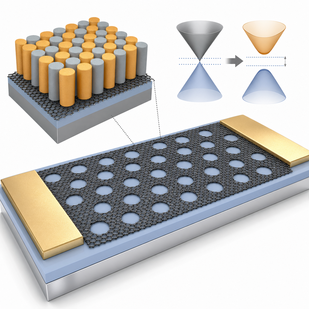
Ultra-high-resolution SEM confirmed a homogeneous, mesh-like NPG structure with an average neck width of ~19 nm across the patterned area. Raman spectroscopy with a 514 nm Ar+ laser was used to verify the sp2 carbon network and assess edge-induced disorder; the appearance and intensity of the D band reflected the newly created nanopore edges, while the 2D/G ratio confirmed retention of single-layer character in the SLG devices. Transport measurements on back-gated NPG FETs fabricated on the 300 nm SiO2/Si stack showed clear semiconducting behavior with a transport gap of approximately 0.08 eV at room temperature, consistent with quantum confinement induced by the sub-20 nm necks. The authors compared single-layer and few-layer NPG FETs, finding that the few-layer devices delivered higher driving currents while still exhibiting gating modulation. Mobility and on/off behavior were reduced relative to pristine graphene, as expected from edge-scattering at the nanomesh boundaries, but the trade-off enabled FET operation impossible with un-patterned graphene.
The demonstration is relevant to flexible electronics, optoelectronics, RF transistors, transparent conducting channels, and chemical and biosensing platforms where a tunable, semiconducting graphene film is needed over large areas. Because PS-b-P4VP self-assembly is solution-processed and parallel, it scales much better than e-beam writing, and the same template strategy can be adapted to other 2D materials such as MoS2 or h-BN. The authors propose further reduction of neck widths to widen the gap toward the 200–300 meV regime needed for room-temperature logic, and integration with high-κ top gates to improve subthreshold swing.
For researchers working on graphene devices, the methodology is portable: a clean, low-defect CVD monolayer is the prerequisite for reproducible nanomesh patterning, and ACS Material's CVD Graphene on Copper Foil — used as the SLG starting material in this study — is available in research and pilot quantities for groups developing nanopatterned graphene FETs, transparent conductive electrodes, and related 2D heterostructures.How ACS Material products were used
- CVD Graphene on Copper Foil (Single-Layer Graphene) (CVD Graphene) — “An SLG material was purchased from ACS Material, USA.”
Product Performance in this StudyThe CVD single-layer graphene from ACS Material served as the base 2D film that was transferred to a SiO2/Si substrate and then nanopatterned by block co-polymer lithography. The starting material enabled clean transfer, successful nanomesh formation with ~19 nm neck widths, and functional FET behavior, including a bandgap opening of ~0.08 eV.
Related product categories
Frequently asked questionsHow does block co-polymer lithography open a bandgap in CVD graphene?
Block co-polymer lithography uses self-assembled polymer domains as an etch template to punch a dense, ordered nanomesh into a continuous graphene film. When the resulting neck widths fall below ~20 nm, lateral quantum confinement of carriers opens a transport bandgap. In this study, PS-b-P4VP templates produced ~19 nm necks in CVD single-layer graphene, yielding a measured bandgap of approximately 0.08 eV at room temperature.
What grade of CVD graphene is best for nanopatterned graphene FET fabrication?
Nanopatterning requires CVD graphene that is continuous, low in defects, and transferable to SiO2/Si without tearing, because every pinhole becomes a yield-limiting defect after etching. Single-layer CVD graphene grown on copper foil and transferred with a PMMA support layer is the standard choice. Few-layer films can be used when higher driving current is needed at the expense of slightly weaker quantum confinement.
Why is a sub-20 nm neck width important for graphene nanomesh transistors?
The bandgap induced by lateral confinement in a graphene nanomesh scales inversely with the neck width. Above ~20 nm the gap is too small to suppress off-state conduction at room temperature, while at ~19 nm a gap of approximately 0.08 eV is achievable. Pushing necks below 10 nm is expected to yield gaps approaching 200–300 meV, the range required for practical logic-level on/off ratios.