-
PET/Silicone Transfer of CVD Graphene - Nankai University, 2013
Jun 04, 2026 | ACS MATERIAL LLCChen, X. et al. (2013). High-Quality and efficient transfer of large-Area graphene films onto different substrates. *Carbon*. https://doi.org/10.1016/j.carbon.2013.01.011
Carbon · 2013
Nankai University researchers used ACS Material CVD graphene on copper foil to develop a fast, low-cost PET/silicone transfer method for large-area graphene.
About this research
Researchers at Nankai University, working in the Key Laboratory of Weak Light Nonlinear Photonics and the Key Laboratory of Functional Polymer Materials, used ACS Material CVD graphene on copper foil (ACS Material Graphene/Cu) to demonstrate a new high-quality, large-area graphene transfer method based on a polyethylene terephthalate (PET)/silicone two-layer carrier. The approach uses purely dispersive adhesion rather than chemical adhesives, transfers films to arbitrary rigid or flexible substrates in seconds at ambient conditions, and allows the PET/silicone carrier to be recycled. Compared with the widely used thermal release tape (TRT) route, the transferred graphene showed a cleaner surface, lower doping, higher optical transmittance, and higher conductivity.
Reliable transfer of CVD graphene from copper foil onto target substrates remains one of the biggest bottlenecks for graphene electronics. The two dominant methods, PMMA-supported transfer and thermal release tape, both have well-known drawbacks: PMMA tends to leave polymer residues, cracks, and tears on large-area films and requires considerable manual skill, while TRT contaminates the graphene surface with acrylic adhesive that degrades sheet resistance and optical transmittance. These residues are particularly damaging for field-effect transistors (FETs), transparent conducting electrodes, photonic devices, and flexible electronics, where doping and surface cleanliness directly determine device performance. A scalable, adhesive-free, low-cost transfer step is therefore central to moving graphene from laboratory demonstrations to industrial-scale optoelectronic and sensing applications.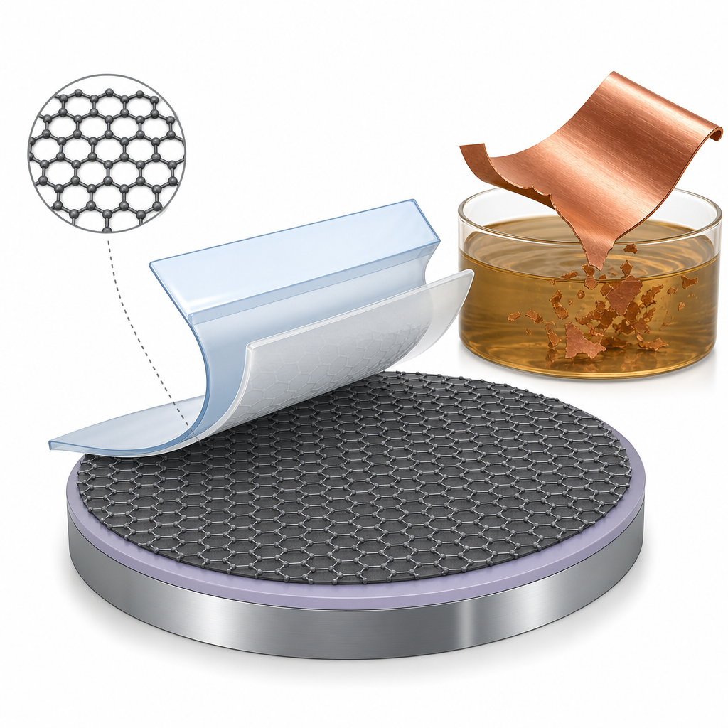
In this work the ACS Material CVD graphene on copper foil functioned as the as-grown source film whose transfer was being studied. The graphene/Cu sample was first flattened between two clean glass slides and then laminated to a commercial PET/silicone film (a Capdase iMAG screen protector with ~100 µm PET and ~60 µm silicone layers) under 0.05 MPa of pressure for 1 h to ensure conformal dispersive adhesion. The underlying copper was etched in 1 M FeCl3 for 1 h, the stack was rinsed with deionized water and then with 10% HCl at 60 °C for 30 min to remove residual Fe3+, dried with N2, laminated onto the target substrate (SiO2/Si wafer with 285 nm oxide, or flexible PET), and finally the PET/silicone carrier was peeled off. For comparison, identical ACS Material graphene/Cu samples were also transferred with thermal release tape. Three-layer films transferred to SiO2/Si were used to fabricate FETs with metal-mask electrodes, followed by vacuum annealing at 120 °C for 1 h.
Characterization with optical microscopy, AFM, Raman mapping (514 nm, 50× objective, 1 µm step over 20 × 20 µm regions), Hall-effect sheet resistance, and HITACHI U-4100 transmittance measurements showed clear advantages for the PET/silicone route. Graphene films transferred by PET/silicone exhibited a cleaner and more continuous surface, with markedly fewer adhesive residues than TRT-transferred counterparts. Raman analysis indicated a lower doping level, while optical transmittance and electrical conductivity were both higher for PET/silicone-transferred films at comparable layer counts. The PET/silicone carrier could be reused four times to transfer successive graphene films, with each cycle still producing clean, continuous coverage, which substantially lowers the per-transfer materials cost. The method was demonstrated on both rigid SiO2/Si substrates and flexible PET without any prior surface treatment of the target substrate, and the entire dispersive-adhesion transfer step at the target substrate took only a few seconds. Three-layer FETs fabricated from the transferred ACS Material graphene operated as expected, confirming that the electronic quality of the graphene survives the transfer.
The demonstrated workflow has direct relevance to flexible transparent electrodes for touch panels, organic light-emitting diodes, and thin-film photovoltaics, where high transmittance and low sheet resistance on plastic substrates are required simultaneously. It is also attractive for graphene FET arrays, biosensors built on flexible plastics, and integrated photonic devices that cannot tolerate adhesive residues from TRT or solvent-based PMMA removal. Because the PET/silicone carrier is a mass-produced screen-protector material and is recyclable, the route is well suited to roll-to-roll style processing of CVD graphene grown on copper. The authors point to FETs and transparent conducting electrodes as immediate device targets, and the dispersive-adhesion concept can in principle be extended to other 2D materials grown on metal foils, such as hexagonal boron nitride and transition metal dichalcogenides.
For researchers developing transparent electrodes, flexible electronics, or graphene-based sensors, the work shows that the quality of the starting CVD graphene film is critical to the final device. ACS Material's CVD Graphene on Copper Foil, used here as the source material, is available in single- and multi-layer formats and is supported by related products including CVD graphene on SiO2, quartz, PET, and Trivial Transfer® Graphene films for groups that prefer a ready-to-transfer format. These offerings give materials and device laboratories a consistent starting point when evaluating new transfer chemistries such as the PET/silicone dispersive-adhesion method reported here.How ACS Material products were used
- CVD Graphene on Copper Foil (CVD Graphene) — “The single-layer and multi-layer graphene on copper foil we used in the experiments were ACS Material Graphene/Cu.”
Product Performance in this StudyThe ACS Material CVD graphene on copper foil served as the starting material whose transfer was being optimized. After transfer with the new PET/silicone method, the graphene retained a clean, continuous surface with low doping, high optical transmittance, and high conductivity, demonstrating that the source material was of sufficient quality for advanced electronic applications.
Related product categories
Frequently asked questionsHow does the PET/silicone method transfer CVD graphene from copper foil?
The PET/silicone film is laminated to graphene grown on copper at 0.05 MPa for one hour using dispersive adhesion. The copper is etched in 1 M FeCl3, residual iron is removed with 10% HCl at 60 °C, and the PET/silicone/graphene stack is then pressed onto a target substrate such as SiO2/Si or flexible PET. Peeling off the PET/silicone in seconds releases a clean, continuous graphene film without any chemical adhesive.
Why does PET/silicone transfer outperform thermal release tape for CVD graphene?
Thermal release tape leaves acrylic adhesive residues on graphene that increase doping and sheet resistance and reduce optical transmittance. The PET/silicone method relies on reversible dispersive adhesion, so no chemical glue contacts the graphene. The resulting films have cleaner, more continuous surfaces, lower Raman-detected doping, higher optical transmittance, and higher electrical conductivity, making them better suited to transparent electrodes and field-effect transistors.
What applications benefit from large-area CVD graphene on copper foil?
Large-area CVD graphene grown on copper foil is the starting material for transparent conducting electrodes in touch panels, OLEDs, and thin-film solar cells, as well as for flexible field-effect transistors, photodetectors, and biosensors. Its combination of high carrier mobility, optical transparency, and mechanical flexibility makes it valuable wherever conventional indium tin oxide is too brittle or too expensive, particularly on plastic and other flexible substrates.