-
Reduced Graphene Oxide Inkjet Sensors - Iowa State University, 2017
May 28, 2026 | ACS MATERIAL LLCHondred, J. A. et al. (2017). High-Resolution Graphene Films for Electrochemical Sensing via Inkjet Maskless Lithography. *ACS Nano*. https://doi.org/10.1021/acsnano.7b03554
Iowa State University · ACS Nano · 2017
Iowa State University used ACS Material reduced graphene oxide to create high-resolution (20 μm) printed graphene films for flexible H2O2 electrochemical sensors.
About this research
Researchers at Iowa State University developed a new patterning technique called inkjet maskless lithography (IML) using completely reduced graphene oxide supplied by ACS Material (catalog GN1P0005, 1-5 μm flake size), achieving printed graphene line widths down to 20 μm - significantly finer than the ~60 μm resolution typical of conventional inkjet-printed graphene. Published in ACS Nano in 2017 by Hondred, Stromberg, Mosher, and Claussen, the work demonstrates that high-resolution flexible graphene circuits can be fabricated without photolithography, stencils, or cleanroom infrastructure. The patterned electrodes were used to build hydrogen peroxide (H2O2) sensors and interdigitated electrode (IDE) arrays for impedance-based sensing.
Scalable manufacturing of flexible printed electronics has surged in importance for energy storage devices, smart packaging, flexible displays, and diagnostic biosensors. Graphene-based inks are particularly attractive because of high electrical and thermal conductivity, mechanical flexibility, chemical robustness, and biocompatibility. However, conventional printing techniques such as screen, gravure, and inkjet printing are typically limited to feature sizes above 50 μm, and finer resolutions traditionally require photolithographic stencils or gravure templates that are costly, slow, and incompatible with rapid prototyping. The IML approach addresses this gap by combining inkjet-printed sacrificial polymer patterns with viscous spin-coated graphene and acetone-based lift-off, making rapid prototyping of flexible graphene circuits possible on substrates ranging from silicon to Kemafoil PET and polyimide.
The ACS Material reduced graphene oxide was the conductive backbone of the entire process. To prepare the printable graphene ink, 150 mg of the as-supplied rGO powder was vortexed in 50 mL of ethanol, mixed with ethyl cellulose binder (25 mg/mL) and terpineol, then probe-sonicated at 70% amplitude for two hours followed by six hours of bath sonication. Ethanol was evaporated to yield a stable graphene ink at 15 mg/mL with viscosity 176.2 cP, well-suited for spin coating. After an inkjet-printed acrylic lacquer negative pattern was applied, this graphene ink was spin-coated at 1000 rpm for 30 s and post-baked at 120 °C for 1 hour to promote adhesion. Acetone lift-off then removed the polymer mask, leaving sharp-edged graphene lines as narrow as 20 μm with heights of approximately 0.4-0.6 μm confirmed by AFM and confocal microscopy.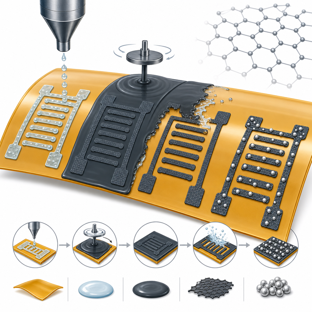
Electrically, the as-patterned graphene had an initial resistance of 135 ± 15 kΩ across a 25 × 3 mm area. Thermal annealing at 1000 °C in nitrogen reduced the resistance to 3.5 ± 0.25 kΩ, while laser annealing - compatible with thermally sensitive PET - brought resistance down to 329 ± 18 Ω, equivalent to a sheet resistance near 90 Ω/sq and conductivity around 26,000 S/m. XPS confirmed dominant sp2/sp3 C-C bonding before annealing and limited oxygen-functional group formation after laser exposure. For H2O2 detection, platinum nanoclusters (25-50 nm) were electrodeposited onto the laser-annealed graphene. Cyclic voltammetry showed peak oxidation at +0.4 V, and amperometric testing yielded a wide linear range from 0.1 to 550 μM (R² = 0.996), sensitivity of 0.21 μM/μA, detection limit of 0.21 ± 0.16 μM, and a 5 s response time. Three IDE designs were characterized by EIS in KCl, with the smallest 50/50 μm finger/spacing geometry showing the largest 21 kΩ impedance response and a double-layer capacitance of approximately 5 nF.
The IML technique opens a route to rapid prototyping of graphene-based flexible electronics without cleanroom infrastructure. Demonstrated applications include non-enzymatic peroxide sensors, impedimetric biosensors, and IDE arrays where smaller feature sizes give higher sensitivity. The authors note that IML is compatible with diverse substrates - silicon, Kemafoil heat-treated PET, clear PET, and polyimide tape - and is not restricted to graphene; silver nanoparticle inks were also successfully patterned. Adjacent application areas the authors flag include energy harvesters, supercapacitors, triboelectric nanogenerators, strain sensors, batteries, and chemical/biological sensors, all of which benefit from scalable roll-to-roll-compatible patterning of high-conductivity nanomaterial films.
For researchers developing printed flexible electronics, biosensors, or interdigitated electrochemical devices, the reduced graphene oxide used here is available from ACS Material and integrates straightforwardly into solution-phase inks. This study provides a useful benchmark for ink formulation, post-bake conditions, and post-deposition laser annealing parameters when working with rGO-based inks on temperature-sensitive flexible substrates. The combination of accessible rGO starting material and a photolithography-free patterning workflow lowers the barrier for academic groups exploring printed graphene electrochemistry.How ACS Material products were used
- Reduced Graphene Oxide (RGO) (Graphene Series) — “Graphene ink (10 mL) was synthesized by first vortexing 150 mg of completely reduced graphene oxide (ACS Material, GN1P0005, 1-5 μm flake size) in 50 mL of ethanol”
Product Performance in this StudyThe reduced graphene oxide served as the conductive nanomaterial in the spin-coatable graphene ink. After IML patterning and laser annealing, the resulting films achieved sheet resistance of ~90 Ω/sq and electrical conductivity of ~26,000 S/m, enabling high-resolution (20 μm) flexible electrochemical sensors.
Related product categories
Frequently asked questionsHow does reduced graphene oxide perform in inkjet maskless lithography for flexible sensors?
Reduced graphene oxide from ACS Material was formulated into a 15 mg/mL spin-coatable ink and patterned with sacrificial polymer lift-off to give 20 μm line widths on flexible PET. After laser annealing, the rGO films reached a sheet resistance near 90 Ω/sq and conductivity around 26,000 S/m, enabling sensitive H2O2 detection with a 0.21 μM detection limit and 5 s response time.
Why is laser annealing important for printed graphene electrodes?
Laser annealing burns off binders and solvents while fusing graphene flakes and creating nano/microstructured surfaces that increase active area. In this study, laser annealing reduced patterned graphene resistance from 135 kΩ to 329 Ω across a 25 × 3 mm area, raising conductivity to roughly 26,000 S/m without damaging thermally sensitive PET substrates - critical for flexible electronics that cannot tolerate furnace processing.
What advantages do smaller interdigitated electrode features offer in electrochemical sensing?
Smaller IDE finger widths and spacings increase the density of collection sites and signal-to-noise ratio. In this work, an IDE with 50 μm fingers and 50 μm spacing produced a 21 kΩ impedance response to KCl concentration changes - far larger than the 4.5 kΩ response from 150/200 μm geometry - demonstrating that finer features made possible by inkjet maskless lithography directly translate into higher sensor sensitivity.