-
Silver Nanowire SWNT/Si Solar Cells - Yale University, 2014
May 21, 2026 | ACS MATERIAL LLCLi, X., Jung, Y., Huang, J., Goh, T., & Taylor, A. D. (2014). Device Area Scale-Up and Improvement of SWNT/Si Solar Cells Using Silver Nanowires. *Advanced Energy Materials*. https://doi.org/10.1002/aenm.201400186
Department of Chemical and Environmental Engineering Yale University New Haven CT 06511 USA · Advanced Energy Materials · 2014
Yale researchers use ACS Material silver nanowires to scale SWNT/Si solar cells to 49 mm² with ~11% efficiency, overcoming series resistance losses.
About this research
Researchers at the Department of Chemical and Environmental Engineering, Yale University, New Haven, used silver nanowires supplied by ACS Material to scale single-walled carbon nanotube (SWNT)/silicon hybrid solar cells to a 49 mm² junction area while preserving ~11% power conversion efficiency, a result previously unattainable for nano-carbon/Si devices at this size. The AgNWs were spin-cast onto the SWNT/n-Si junction to form a bilayer AgNW/SWNT top window, drastically lowering parasitic series resistance and rescuing the fill factor that normally collapses upon device scale-up. The paper, published in Advanced Energy Materials in 2014, directly compares its 49 mm² cell against literature reports where similar-sized devices delivered only ~1.3% efficiency.
Nano-carbon/Si hybrid solar cells (using SWNT films or graphene as the transparent emitter on n-type Si) are attractive because they combine the high intrinsic photovoltaic efficiency of Si with low-temperature, solution-processable junction formation. The literature reports efficiencies up to 15% for cells under ~15 mm² in area. However, total resistive power loss scales with the product of series resistance and device area (R_s·A), so large-area cells suffer collapsing fill factors and current densities. Previous attempts to add metal grids onto thin nano-carbon emitters caused electrical shorts because evaporated metal could penetrate the porous, ultrathin (≈10 nm) SWNT films and short to the underlying Si. A non-damaging, solution-processable conductive overlayer was therefore needed to make CNT/Si and graphene/Si photovoltaics commercially viable at module-relevant areas.
The authors first prepared dense, transparent p-type SWNT films (8–12 nm thick, verified by AFM) by chlorosulfonic acid dispersion and slide-casting, then transferred them onto pre-patterned, metalized n-Si wafers. Onto this fragile SWNT emitter they drop-cast and spin-coated silver nanowires obtained from ACS Material at 1000–2000 rpm. The cited AgNWs had diameters of approximately 50–75 nm, characterized by SEM, which is much larger than the 1–5 nm pores of the SWNT thin film, ensuring that the nanowires sat on top of the SWNT network rather than penetrating to short the Si surface. The AgNWs were used as-supplied as a solution-processable network electrode, eliminating the need for physical vapor deposition. The resulting AgNW/SWNT bilayer combined the photocarrier separation function of the SWNT emitter with the high lateral conductance of the AgNW network.Scaling carbon/Si and 2D-material/Si photovoltaics to module-relevant areas depends on a solution-processable, low-resistance top electrode that will not short the fragile junction. In this Yale study, spin-cast silver nanowires (50–75 nm) formed an AgNW/SWNT bilayer that cut sheet resistance from 434 to about 10 ohm/sq and preserved roughly 11% efficiency at a 49 mm² junction. Explore our Silver Nanowires (Nanowire Series) to build large-area hybrid solar cells, transparent conductive electrodes, and printable PV modules.
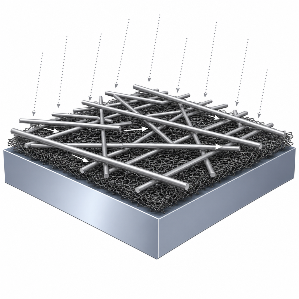
The AgNW overlay produced dramatic optoelectronic gains. Sheet resistance dropped from 434 ohm/sq (bare SWNT) to 9.97 ohm/sq (AgNW/SWNT bilayer), a more than 40× reduction, matching the ~10–20 ohm/sq range of conventional Si emitter layers. The specular optical transmittance fell from 90.2% to 68.8% at 550 nm; however, the authors note that AgNW networks scatter approximately 10% of light forward, partly recovering this loss as diffuse transmittance useful for absorption. With this electrode, the champion 49 mm² SWNT/Si cell achieved a power conversion efficiency of 10.8% with J_sc = 31.0 mA cm⁻², V_oc = 0.51 V, and FF = 0.69. By contrast, prior 49 mm² CNT/Si cells reached only 1.3% efficiency with FF = 0.19. Even at smaller areas (9 mm²), the AgNW addition improved performance over bare SWNT/Si references in the literature. The bilayer improvement scaled with cell area, exactly the region where series-resistance losses dominate, confirming the mechanism of mitigating R_s·A power loss.
This work has clear implications for low-cost, large-area photovoltaics, where Si remains the gold-standard absorber but conventional doped-emitter processing is expensive. Solution-processable AgNW/SWNT bilayer electrodes enable wafer-area hybrid cells without requiring evaporated metal grids, ITO sputtering, or high-temperature doping diffusion. The strategy is also transferable to graphene/Si and other 2D-material/Si junctions, to flexible and semitransparent PV modules, and to broader optoelectronic devices such as transparent conductive films for touchscreens, OLEDs, and large-area photodetectors where porous nanocarbon emitters need a robust conductive overlayer. Future scale-up to true module-size wafers will hinge on AgNW length, junction welding, and encapsulation against silver migration.
For researchers replicating or extending this device architecture, silver nanowires of comparable dimensions are available from ACS Material under the Nanowire Series, alongside SWNT and graphene products that map to other layers of this type of cell. The combination is well suited to teams investigating scale-up of carbon-based hybrid photovoltaics, transparent electrodes for flexible electronics, and printable solar modules.How ACS Material products were used
- Silver Nanowires (AgNWs) (Nanowire Series) — “we drop cast AgNWs (ACS Material) by spin coating (1000 to 2000 rpm)”
Product Performance in this StudyThe ACS Material silver nanowires, spin-cast onto the SWNT/Si junction, formed a conductive top window that drastically reduced sheet resistance (from 434 to 9.97 ohm/sq) and enabled an unprecedented ~11% efficiency at a 49 mm² junction area.
Related product categories
Frequently asked questionsHow do silver nanowires improve large-area SWNT/Si solar cells?
Silver nanowires spin-cast on top of the SWNT emitter form a conductive AgNW/SWNT bilayer that dramatically reduces lateral sheet resistance, from 434 ohm/sq to about 9.97 ohm/sq. Because resistive power loss scales as R_s·A, lowering sheet resistance is essential when scaling up cell area. In this Yale study, the AgNW overlayer enabled a 49 mm² SWNT/Si cell to reach roughly 11% efficiency, versus 1.3% for prior same-area cells.
Why use silver nanowires instead of evaporated metal grids on carbon nanotube solar cells?
Evaporated metal can penetrate the porous, ultra-thin SWNT or graphene emitter (only ~10 nm thick with 1–5 nm pores) and short directly to the silicon underneath. Solution-cast silver nanowires with 50–75 nm diameters sit on top of the SWNT film without penetrating its pores, preserving the p-n junction. Spin coating is also low-cost, room-temperature, and compatible with flexible substrates, unlike physical vapor deposition.
What efficiency did the AgNW/SWNT/Si solar cell achieve and at what device area?
The champion device achieved a power conversion efficiency of 10.8% with a short-circuit current density of 31.0 mA cm⁻², open-circuit voltage of 0.51 V, and fill factor of 0.69 at a junction area of 49 mm². This is the largest reported nano-carbon/Si solar cell with greater than 10% efficiency, compared to a prior 1.3% efficiency at the same 49 mm² area without the silver nanowire overlay.