-
SiO2/Si Substrate for Graphene AFM Imaging - USTC, 2024
Jun 03, 2026 | ACS MATERIAL LLCMa, C. et al. (2024). Shear anisotropy domains on graphene revealed by in-plane elastic imaging. *ACS Nano*. https://doi.org/10.1021/acsnano.4c04368
University of Science and Technology of China · ACS Nano · 2024
USTC researchers used an ACS Material SiO2/Si substrate to image shear anisotropy domains on exfoliated graphene by torsional resonance AFM in 2024.
About this research
Researchers at the University of Science and Technology of China used an ACS Material LLC SiO2/Si substrate (90 nm thermal oxide) to support mechanically exfoliated graphene and graphite flakes and, by employing torsional resonance atomic force microscopy (TR-AFM), demonstrated that the universally observed 180°-periodic domains on graphene are of in-plane elastic (shear) anisotropy rather than friction anisotropy. The study, published in ACS Nano in 2024, combined in-plane elastic imaging, transverse shear microscopy (TSM), contact-resonance AFM, and conventional friction force microscopy to disentangle the long-debated physical origin of these domains. The team further showed that the domains originate from self-assembled environmental adsorbates, with the densely packed molecular backbone defining the major axis of each domain's shear anisotropy.
The origin and mechanism of anisotropic domains on graphene and other 2D crystals have remained controversial for over a decade. Since their first report by friction force microscopy, the domains were widely labeled as "friction anisotropy," but competing explanations attributed them either to periodic substrate-induced ripples in the 2D sheet or to self-assembled adsorbate stripes. Resolving this ambiguity matters for tribology, where graphene is studied as a solid lubricant, and for micro- and nanoelectromechanical systems (MEMS/NEMS) where surface forces dominate. A quantitative understanding of the elastic versus frictional nature of these domains informs how 2D materials behave under shear, how contamination self-organizes on van der Waals surfaces, and how surface anisotropy can be measured and even manipulated at the nanoscale.
The ACS Material SiO2/Si substrate, with its 90 nm oxide layer, was the primary support for the exfoliated samples. Graphite and graphene flakes were mechanically exfoliated and transferred onto these substrates, then kept in gel boxes and measured at room temperature and humidity. The flat, well-characterized oxide surface allowed graphene to be located optically with a built-in camera and gave the contrast reference needed to distinguish supported graphene from the bare substrate by contact-resonance AFM, which detected the larger indentation modulus of monolayer graphene. The substrate also enabled thickness determination from folded or stacked regions. A comparison sample from a different supplier on similar SiO2/Si gave equivalent observations, confirming the substrate's suitability. AFM measurements used a Dimension Icon system with a rotational sample stage and silicon ContAl-G cantilevers (nominal radius 10 nm, spring constant 0.2 N/m), operated at soft contacts with tip loads of 5–11 nN. The substrate's stability under repeated rotation, imaging, and tip-writing experiments was essential to the multi-angle anisotropy mapping.
The TR-AFM imaging revealed domains spanning a few to tens of micrometers with three distinct contrast levels, invisible in topography. Monolayer thickness was measured at roughly 359–361 pm and bilayer at 344 pm above the monolayer. Rotating the sample in roughly 12° steps showed approximately 180° periodicity in both TR-AFM and TSM signals, with adjacent domains shifted by about 60°, consistent with prior reports. Quantitative in-plane elastic mapping yielded torsional resonance frequencies of 204.3 ± 0.5 kHz (α), 204.0 ± 0.1 kHz (β), and 203.6 ± 0.2 kHz (γ), translating to lateral (shear) contact stiffnesses of 2.81 ± 0.97, 2.42 ± 0.27, and 1.55 ± 0.38 N/m respectively, using a cantilever lateral stiffness of about 177.8 N/m. TR-AFM Q-value maps gave 31.1 ± 17.6, 38.3 ± 2.0, and 51.0 ± 4.5 for the three domains, indicating distinct in-plane viscoelastic anisotropy. Crucially, the domains were clearly resolved by TR-AFM and TSM but nearly invisible by contact-resonance AFM and only weakly visible by friction force microscopy, proving the anisotropy is in-plane elastic, not frictional. Tip-writing at soft loads created and erased domains depending on scan direction, and domains extended across wrinkles unchanged, supporting the adsorbate-stripe origin with stripe orientations aligned to the major shear axes.
This work provides a quantitative framework for understanding anisotropic domains on graphene, graphite, and other 2D materials, and establishes TR-AFM as a tool for in-plane elastic and viscoelastic imaging of organic molecular crystals and adsorbate layers. The findings are relevant to nanotribology, solid lubrication, and the design of MEMS/NEMS where surface contamination and shear response govern performance. By clarifying that environmental adsorbates self-assemble into ordered, anisotropic stripes on van der Waals surfaces, the study also informs efforts to control surface cleanliness and friction in 2D-material devices. The authors point toward complementary finite-element and molecular-dynamics modeling and detailed chemical identification of the adsorbates as natural follow-up directions.
For researchers working on 2D materials, nanotribology, or scanning-probe characterization, the well-defined SiO2/Si substrate used here is the kind of flat, oxide-coated support available from ACS Material's CVD graphene and substrate offerings. A reproducible, optically transparent-contrast substrate of known oxide thickness is a practical prerequisite for exfoliation, optical identification, and quantitative elastic imaging of graphene. The substrate performed as expected in this study, supporting stable mono- and multilayer samples through repeated rotation and tip-manipulation experiments without interfering with the elastic-domain measurements.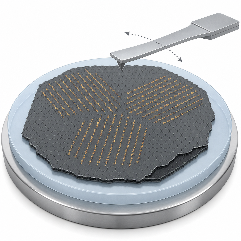
How ACS Material products were used
- SiO2/Si substrate (90 nm thick oxide layer) (CVD Graphene) — “lying on a SiO2/Si substrate, which has a 90 nm thick oxide layer (ACS Material LLC, Pasadena, CA)”
Product Performance in this Study
The ACS Material SiO2/Si substrate (90 nm oxide) served as the supporting substrate onto which mechanically exfoliated graphene and graphite flakes were transferred. It provided a flat, well-characterized surface enabling clear optical location and high-contrast in-plane elastic imaging of the anisotropic domains.
Related product categories
Frequently asked questions
Why is a SiO2/Si substrate with a 90 nm oxide layer used for graphene AFM imaging?
A SiO2/Si substrate with a defined thermal oxide thickness provides a flat, stable support that lets researchers locate exfoliated graphene optically and distinguish it from the bare substrate by elastic imaging. In this study the 90 nm oxide enabled clear contrast in contact-resonance AFM, since monolayer graphene has a larger indentation modulus than the oxide, and supported repeated rotation and tip-writing experiments.
What are shear anisotropy domains on graphene?
Shear anisotropy domains are regions on graphene showing 180°-periodic variation in their in-plane elastic (shear) response. This study used torsional resonance AFM to show these domains are elastic rather than frictional in origin, with measured lateral contact stiffnesses of 1.55 to 2.81 N/m across domains, arising from self-assembled environmental adsorbates whose molecular backbone sets each domain's major shear axis.
How does torsional resonance AFM distinguish elastic anisotropy from friction on graphene?
Torsional resonance AFM excites a cantilever torsional mode in contact, probing in-plane elastic and viscoelastic properties. In this work the domains were clearly resolved by TR-AFM and transverse shear microscopy but nearly invisible by contact-resonance AFM and only weakly seen by friction force microscopy. This contrast proves the domain anisotropy is in-plane elastic rather than frictional, resolving a long-standing labeling debate.