-
Suspended CVD Graphene Anode for Vacuum Nanoelectronics - University of Pittsburgh, 2014
Jul 07, 2026 | ACS MATERIAL LLCSrisonphan, S., Kim, M., & Kim, H. K. (2014). Space charge neutralization by electron-transparent suspended graphene. *Scientific Reports*. https://doi.org/10.1038/srep03764
Scientific Reports · 2014
University of Pittsburgh researchers used ACS Material CVD graphene on Cu foil as a suspended anode, neutralizing space charge and surpassing Child-Langmuir limits.
About this research
Researchers at the University of Pittsburgh demonstrated that a suspended monolayer of CVD graphene on copper foil, purchased from ACS Material, can serve as an electron-transparent anode that neutralizes space charge in a nanoscale vacuum channel and pushes emission currents beyond the Child-Langmuir limit. Published in Scientific Reports in 2014 by Srisonphan, Kim, and Kim, the study fabricated a graphene/SiO2/Si (GOS) device in which the suspended graphene sits above a focused-ion-beam-etched void channel. Under forward bias, a two-dimensional electron gas at the SiO2/Si interface emits ballistically across the void, with less than 0.1% of the impinging low-energy (~3 eV) electrons captured at the graphene edge. The result reframes how 2D materials interact with out-of-plane electron transport.
Vacuum nanoelectronics is undergoing a revival as researchers seek to combine the speed and radiation hardness of vacuum tubes with the integration density of solid-state devices. A persistent obstacle is the space-charge-limited current described by the Child-Langmuir law, which caps the achievable current density once emitted electrons accumulate in the channel and electrostatically suppress further emission. Conventional grid electrodes intercept too many electrons to act as effective space-charge compensators at low voltages. A 2D atomic membrane that is conductive in-plane yet transmissive to low-energy electrons out-of-plane offers a fundamentally new design knob, and graphene is the natural candidate because its damage threshold corresponds to electron energies above 80 keV, well above the few-volt regime of interest.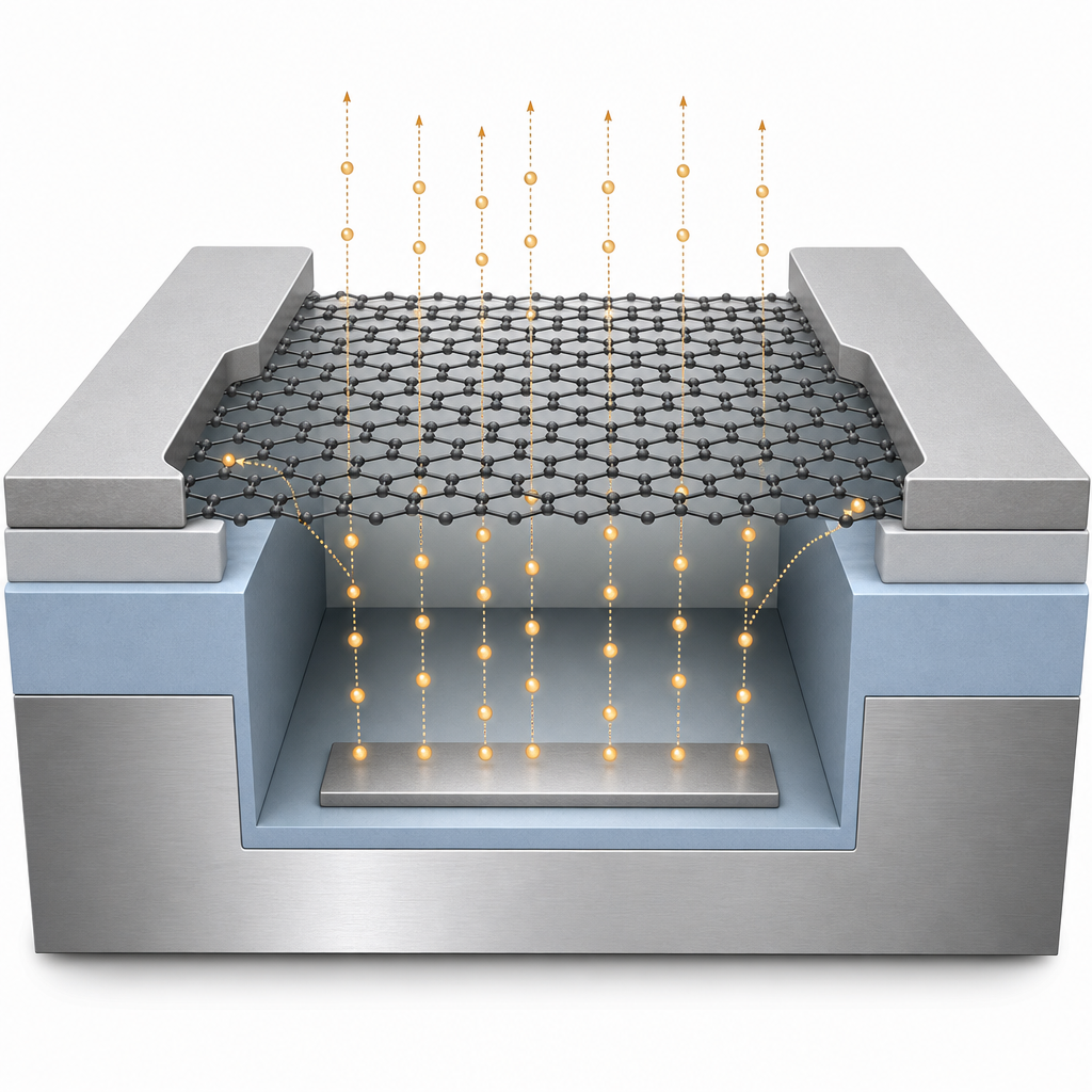
The ACS Material CVD graphene was grown on 25-micrometer-thick copper foil and transferred onto a SiO2 (≈23 nm)/n-Si (5 Ω-cm) substrate that had been patterned with nano-void channels by FIB etching or by photolithography and inductively-coupled-plasma reactive-ion etching. Square wells (0.5 × 0.5 μm cross-section, 1 μm deep) and longer trenches (500–1000 nm deep, 8–10 μm length) were prepared, and the monolayer graphene was placed across the openings to form a freely suspended membrane confirmed by electron microscopy. An aluminum ohmic contact was deposited on the back of the silicon and annealed at 350 °C. After transfer, the samples were dried at 70 °C for two hours to remove moisture from the void channel. In the resulting GOS structure, the graphene acted as the anode while the n-Si substrate served as the cathode emitting the 2D electron gas.
Electrical measurements with an HP4145B semiconductor parameter analyzer revealed that the suspended graphene is highly transparent to very low energy electrons: only a small fraction (<0.1%) of the impinging electrons were captured, consistent with the de Broglie wavelength at <10 eV being larger than the graphene lattice spacing and with the dominance of weak inelastic scattering channels. The captured charges induce a 2D hole system in the graphene, which electrostatically neutralizes the space charge accumulating in the void channel. With this compensation, the 2D electron gas at the SiO2/Si interface emits into the air channel at biases of order 1 V and reaches current densities approaching 10^5 A/cm^2, far exceeding the Child-Langmuir space-charge-limited prediction. Channel lengths of 10–20 nm yield estimated electron transit times of 10–100 fs, with travel essentially scattering-free because the channel is shorter than the ~60 nm mean free path of electrons in air. Together, these numbers establish the suspended graphene anode as both transparent and active: it does not block the beam, yet its induced hole charge restructures the channel potential.
The findings point toward a new class of low-voltage nanoscale vacuum transistors, ballistic electron sources, and high-frequency emitters that exploit graphene as a transmissive grid. Because the graphene is undamaged at these energies, devices can be operated continuously without electrode erosion, an advantage over conventional field-emitter arrays. Applications include high-speed analog electronics, terahertz sources, vacuum-channel logic, and radiation-tolerant circuits for aerospace and nuclear environments. The same architecture can be extended to other 2D anodes such as hexagonal boron nitride and transition-metal dichalcogenide membranes for engineered work functions, and to heterostructures that combine electron-transparent and selectively absorbing layers for energy-resolved electron detection.
For researchers building suspended 2D-material devices, the practical lesson is that the quality and transferability of the starting graphene are decisive: the membrane must remain flat across submicron openings and electrically continuous over the entire channel array. CVD graphene on copper foil from ACS Material, used here, is available to groups working on vacuum nanoelectronics, electron-transparent grids, and 2D heterostructure platforms. The catalog also offers PMMA-coated and pre-transferred variants that can shorten process development for similar nano-void-channel devices.How ACS Material products were used
- CVD Graphene on Copper Foil (CVD Graphene) — “a monolayer graphene (CVD grown on 25-mm-thick Cu foil: purchased from ACS Material) was transferred to the trench-etched SiO2/Si substrate”
Product Performance in this StudyThe CVD monolayer graphene served as the suspended anode over a nano-void channel and functioned as an electron-transparent membrane, enabling the central observation of space-charge neutralization and very low-energy electron transmission.
Related product categories
Frequently asked questionsWhy is CVD graphene a good electron-transparent anode for vacuum nanoelectronics?
Monolayer CVD graphene is a single atomic layer with a damage threshold corresponding to electron energies above 80 keV, so few-volt electrons cause no structural harm. At energies below 10 eV, the de Broglie wavelength exceeds the graphene lattice spacing, suppressing diffraction and allowing the membrane to transmit more than 99.9% of impinging electrons while remaining electrically conductive in-plane as an anode.
How does a suspended graphene anode surpass the Child-Langmuir space-charge limit?
Electrons captured at the graphene edge induce a 2D hole system that electrostatically compensates the accumulating electron space charge inside the nanoscale void channel. With the space charge neutralized, the cathode 2D electron gas at the SiO2/Si interface continues to emit at low bias, reaching current densities near 10^5 A/cm^2 and well exceeding the classical Child-Langmuir prediction for the same geometry.
What graphene grade is suitable for suspended membrane devices over nano-void channels?
Monolayer CVD graphene grown on copper foil is the standard choice because it can be wet-transferred onto pre-patterned SiO2/Si substrates and remain flat across submicron openings. ACS Material supplies this grade on 25-micrometer Cu foil, as used in the Pittsburgh study. PMMA-coated variants are useful when extra mechanical support during transfer over nano-trenches is needed.